Silicon carbide UMOSFET device cellular structure with surge voltage self-inhibiting and self-overvoltage protection

An overvoltage protection and surge voltage technology, which is applied in the direction of electrical components, semiconductor devices, circuits, etc., can solve the problems of failure of gate structure and electrode ohmic contact area, Problems such as breakdown failure in the channel region of the device can reduce the buffer circuit and snubber circuit structure, avoid device damage and reliability loss, and reduce the effect of components

Inactive Publication Date: 2017-05-31
BEIJING CENTURY GOLDRAY SEMICON CO LTD
View PDF3 Cites 3 Cited by
  • Summary
  • Abstract
  • Description
  • Claims
  • Application Information

AI Technical Summary

Problems solved by technology

[0004] However, there are still several problems in the actual fabrication and application of SiC UMOSFETs: 1) The high electric field in the SiC drift region leads to a high electric field on the gate oxide layer, which is exacerbated at the groove corners, resulting in high drain voltages. Rapid breakdown of the gate oxide layer; poor tolerance to electrostatic effects in harsh environments and high-voltage spikes in the circuit; 2) Since SiC power MOSFETs are mainly used in high-voltage, high-frequency, and high-current fields, the parasitic parameters in the circuit will make the high-frequency During the switching process, spikes such as overshoot are generated, such as figure 2 As shown, the transient overvoltage on the current path of the device is caused and the loss of the switching process is increased at the same time; or a large surge voltage is formed due to changes in power loads, etc. Therefore, MOSFET anti-surge voltage capability and overvoltage protection are also very important
Because the existing MOSFET devices do not have anti-surge voltage self-suppression and overvoltage protection capabilities, it is often necessary to design complex snubber circuits, surge voltage suppression circuits and overvoltage protection circuits in practical applications, such as image 3 shown
However, this external matching suppression and overvoltage protection circuit often has a time delay, and the high-frequency peak voltage surge in the actual switching process is still borne by the device itself, which sometimes leads to breakdown failure in the channel region of the device and gate failure. Gradual failure of structures and electrode ohmic contact areas, causing device reliability issues

Method used


Image

  • Silicon carbide UMOSFET device cellular structure with surge voltage self-inhibiting and self-overvoltage protection
  • Silicon carbide UMOSFET device cellular structure with surge voltage self-inhibiting and self-overvoltage protection
  • Silicon carbide UMOSFET device cellular structure with surge voltage self-inhibiting and self-overvoltage protection

Examples


Embodiment Construction

[0019] The present invention will now be described more fully with reference to the accompanying drawings, in which exemplary embodiments of the invention are shown. This invention may, however, be embodied in many different forms and should not be construed as limited to the exemplary embodiments set forth herein. Rather, these embodiments are provided so that this disclosure will be thorough and complete, and will fully convey the scope of the invention to those skilled in the art.

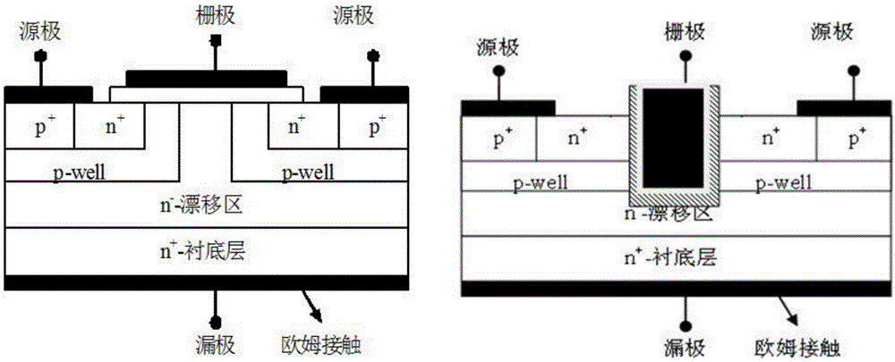
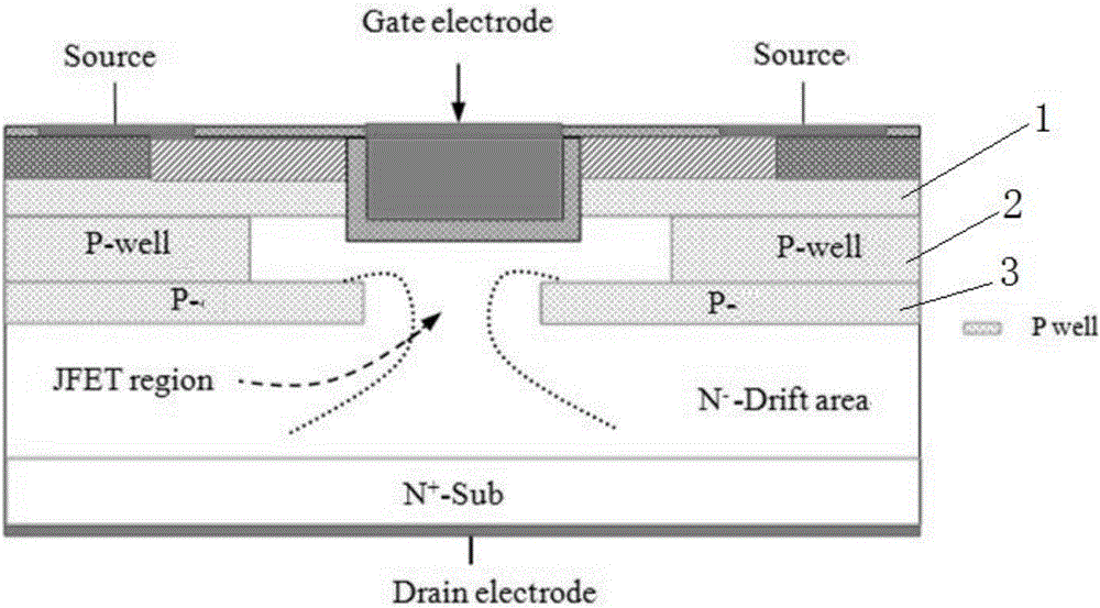
[0020] Such as image 3 As shown, the present invention provides a silicon carbide UMOSFET device cell structure with surge voltage self-suppression and self-overvoltage protection. The p-well area of ​​the cell structure is divided into three layers, wherein the uppermost layer 1 is located at the bottom of the U-shaped groove The left and right sides are in contact with the U-shaped groove; the middle layer 2 and the bottom layer 3 are composed of two parts respectively arranged on the left a...


PUM


Abstract

The invention discloses a silicon carbide UMOSFET device cellular structure with surge voltage self-inhibiting and self-overvoltage protection. A p-well area of the cellular structure is divided into three layers; the topmost layer is located at the left side and the right side of a U-shaped slot, and is in contact with the U-shaped slot; each of the middle layer and the bottommost layer is formed by two parts respectively arranged on the left side and the right side of the cellular structure; the left part and the right part of the middle layer and the bottommost layer are not in contact with each other; the distance between the left and right parts of the middle layer and a vertical middle axle line of the cellular structure is larger than the distance between the left and right parts of the bottommost layer and the vertical middle axle line of the cellular structure; a JFET structure is introduced onto a drain electrode current path of the cellular structure. According to the silicon carbide UMOSFET device cellular structure with surge voltageself-inhibiting and self-overvoltage protection provided by the invention, the JFET structure is specifically introduced onto the drain electrode current path, so that device on resistance and a self-locking protection effect are automatically adjusted, and meanwhile, a smaller device cellular size can be maintained.

Description

technical field [0001] The invention belongs to the technical field of H01L 27 / 00 semiconductor devices, and in particular relates to a silicon carbide UMOSFET device cell structure with surge voltage self-suppression and self-overvoltage protection. Background technique [0002] Because of its excellent characteristics, SiC material has a strong appeal in high power, and has become one of the ideal materials for high-performance power MOSFETs. SiC vertical power MOSFET devices mainly include lateral double-diffused DMOSFET and UMOSFET with vertical gate groove structure, such as figure 1 shown. The DMOSFET structure adopts planar diffusion technology, uses refractory materials, such as polysilicon gate as a mask, and defines the P base region and N+ source region with the edge of the polysilicon gate. The name of DMOS comes from this double diffusion process. The surface channel region is formed by using the side diffusion difference between the P-type base region and th...

Claims


Application Information

Patent Timeline
Patent Type & Authority Applications(China)
IPC IPC(8): H01L29/78H01L29/06
CPCH01L29/0696H01L29/7803H01L29/7813H01L29/1095H01L29/1608
Inventor 袁俊倪炜江张敬伟李明山牛喜平徐妙玲孙安信
Owner BEIJING CENTURY GOLDRAY SEMICON CO LTD
Why Eureka
Try Eureka