Multi-band light perfect absorber on basis of metal film layer-semiconductor resonant cavity composite structures

A metal film layer, composite structure technology, applied in the fields of nanophotonics and optoelectronic materials, can solve the problem of not being able to have perfect light absorption and perfect conductance response at the same time

Inactive Publication Date: 2017-05-31
JIANGXI NORMAL UNIV
View PDF6 Cites 14 Cited by
  • Summary
  • Abstract
  • Description
  • Claims
  • Application Information

AI Technical Summary

Problems solved by technology

Therefore, the design and realization of a multi-band optical perfect absorber based on the metal film layer-semiconductor resonant cavity composite structure will have very important practical significance for solving the problem that existing research systems and invented structures cannot simultaneously have perfect optical absorption and perfect conductance response. and application value

Method used


Image

  • Multi-band light perfect absorber on basis of metal film layer-semiconductor resonant cavity composite structures
  • Multi-band light perfect absorber on basis of metal film layer-semiconductor resonant cavity composite structures
  • Multi-band light perfect absorber on basis of metal film layer-semiconductor resonant cavity composite structures

Examples


Embodiment 1

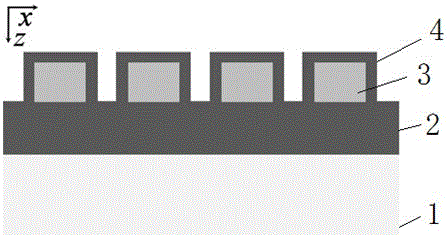
[0039] Embodiment 1: see figure 1 Shown is the longitudinal cross-sectional schematic diagram of the multi-band optical perfect absorber based on the metal film layer-semiconductor resonant cavity composite structure in this embodiment, which includes a substrate, a metal reflective layer, a semiconductor resonant cavity layer and a metal resonant cavity layer arranged in sequence from bottom to top. film layer. The metal light-reflecting layer in this embodiment constitutes the reflective and opaque layer of the absorber, and the semiconductor resonant cavity layer and the metal film layer constitute the resonant composite structural unit that the absorber produces a strong electromagnetic resonance effect. By optimizing the design such as figure 2 The shown semiconductor resonant cavity layer and metal film layer can obtain perfect absorption of multi-band light of preset wavelength bands. At the same time, the metal film layer can be used as a perfect conductive layer to ...

Embodiment 2

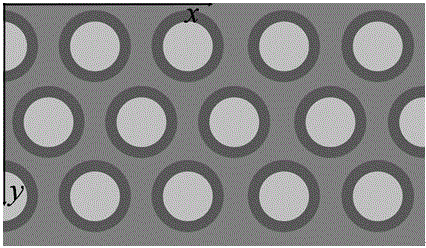
[0040] Embodiment 2: the longitudinal sectional view of this embodiment can refer to figure 1 , top view diagram see figure 2 , which differs from Embodiment 1 mainly in that the semiconductor resonant cavity layer in this embodiment forms a two-dimensional periodic array structure. participate image 3 The multi-band light perfect absorption formed by it can form perfect light absorption for incident light with different polarization directions, thereby further improving the light absorption performance and photoelectric response efficiency of the absorber under different electromagnetic polarization environments.

Embodiment 3

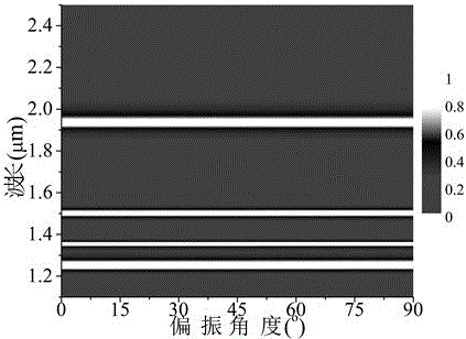
[0041] Embodiment 3: see Figure 4 Shown is the light absorption diagram of the multi-band optical perfect absorber based on the metal film layer-semiconductor resonant cavity composite structure in this embodiment. The metal material is gold, the semiconductor material is single crystal silicon, and the thickness of the metal substrate and the thickness of the metal film layer are 100nm and 20nm respectively. The semiconductor resonant cavity is a cylindrical structure with a diameter of 400nm and a cylinder height of 380nm. The semiconductor resonant cavity array is arranged in a triangle, and the period size is 500nm. In the near-infrared band, there are four light absorption peaks, and the maximum light absorption rate reaches 98%. The minimum absorption rate also exceeds 92%. Such an excellent light absorption effect is obtained on the basis that the structure is 100% covered by a 20nm-thick metal film layer, which forms a huge contrast with the inherent high light ref...


PUM


Abstract

The invention discloses a multi-band light perfect absorber on the basis of metal film layer-semiconductor resonant cavity composite structures. According to the technical scheme, the multi-band light perfect absorber has the advantages that the multi-band light perfect absorber is a novel multi-band light absorber, incident light is free of influence of high-reflection continuous metal layers which cover integral structures, and accordingly light can be perfectly absorbed by the multi-band light perfect absorber with the absorption rate of 99%; the metal film layers with excellent conductivity electric characteristics wrap the structures of the multi-band light perfect absorber by 100%, and accordingly the multi-band light perfect absorber is perfect in electric response in the aspect of conductivity characteristics such as resistance lower than 0.1 ohm / sq; the shortcoming of deficiency of simultaneous high light absorption and high conductivity characteristics of structural designs in the prior art can be overcome by the aid of excellent optical and electric characteristics of the multi-band light perfect absorber, introduced semiconductor materials are combined with the multi-band light perfect absorber, accordingly, the multi-band light perfect absorber is compact in structure and easy to process and prepare and has an excellent application prospect in development of high-performance photoelectric detection, thermal electron excitation and collection, multi-band filtering and imaging and the like, immeasurable effects can be realized by the multi-band light perfect absorber, and the like.

Description

technical field [0001] The invention relates to the fields of nanophotonics and optoelectronic materials, and in particular to a multi-band light perfect absorber based on a metal film layer-semiconductor resonant cavity composite structure. Background technique [0002] The concept of surface plasmons is the collective oscillation caused by metal free electrons under the irradiation of external light waves, which leads to the localization of electromagnetic fields on the metal surface and produces an electric field enhancement effect, thereby forming surface plasmons (Surface plasmons). SPR-based metal structures can be used as core components in the fields of energy, photodetection, biology, and medicine. [0003] The optical perfect absorber is an essential component to realize high-efficiency spectral absorption and photoelectric detection. It can realize the absorption of light wave energy in a specific band or multiple band spectral ranges. The principle is generally p...

Claims


Application Information

Patent Timeline
Patent Type & Authority Applications(China)
IPC IPC(8): H01L31/02H01L31/0232H01L31/0352
CPCH01L31/02H01L31/02327H01L31/0352
Inventor 刘正奇刘桂强
Owner JIANGXI NORMAL UNIV
Why Eureka
Try Eureka