Preparation method of deposited cspbbr3 nanosheet thin film photodetector

A technology of photodetectors and nanosheets, which is applied in the direction of circuits, electrical components, semiconductor devices, etc., can solve the problems of unsuitable large-area preparation of thin films and limited volume of centrifuge tubes, so as to ensure large-area uniformity and compactness, The method is flexible and controllable, and the effect of improving performance

Inactive Publication Date: 2018-09-04
XI AN JIAOTONG UNIV
View PDF9 Cites 1 Cited by
  • Summary
  • Abstract
  • Description
  • Claims
  • Application Information

AI Technical Summary

Problems solved by technology

However, the centrifugal deposition method is limited by the volume of the centrifuge tube, which is not suitable for the large-area preparation of the film. At the same time, it will be affected by factors such as the nature of the dispersion solution and the centrifugal speed, so that the thickness of the deposited film is not easy to increase with the total amount of quantum dots added. do linear adjustment

Method used


Image

  • Preparation method of deposited cspbbr3 nanosheet thin film photodetector
  • Preparation method of deposited cspbbr3 nanosheet thin film photodetector
  • Preparation method of deposited cspbbr3 nanosheet thin film photodetector

Examples


Embodiment 1

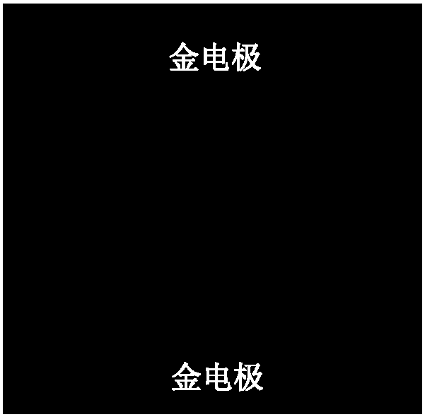
[0029] 1) Prepare patterned gold interdigitated electrodes with a pitch of 25 microns on the silicon substrate by photolithography, such as figure 1 shown;

[0030] 2) CsPbBr with a concentration of 10mg / mL 3 The nanosheet octadecene solution was centrifuged twice at 500 rpm, and finally dispersed into n-hexane to obtain CsPbBr 3 Nanosheet n-hexane dispersion, for later use;

[0031] 3) Put the container on the shock-absorbing table, then arrange 10 pieces of gold interdigitated electrodes in a circular beaker with a diameter of 2.2cm, and add 2mL of 0.05g / mL CsPbBr 3 Nanosheet n-hexane dispersion;

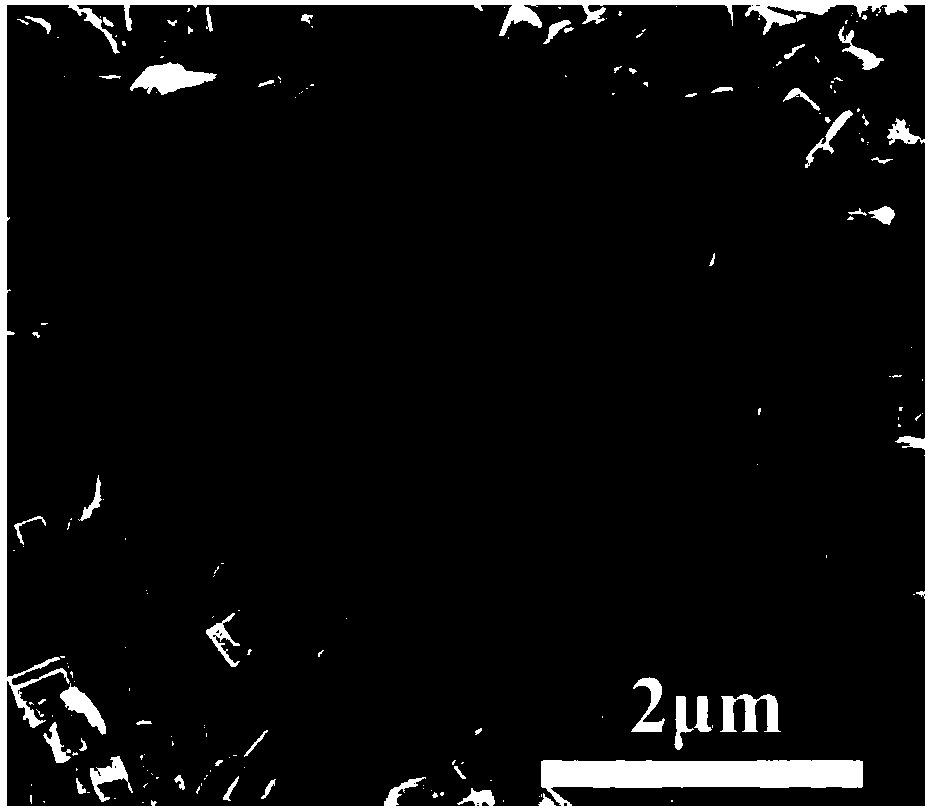
[0032] 4) Place the container open and keep it at 25°C until the n-hexane is completely evaporated to obtain deposited CsPbBr 3 Gold interdigitated electrodes of nanosheets;

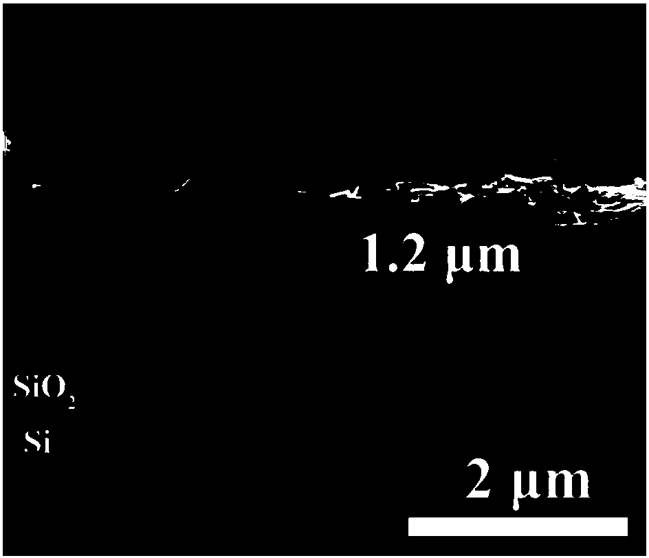
[0033] 5) will deposit CsPbBr 3 The gold interdigitated electrode of the nanosheet is transferred to a hot stage at 90°C in air, and thermally annealed for 0.5h to obtain a chip;

[0034] 6) Connect t...

Embodiment 2

[0036] 1) Prepare patterned gold interdigitated electrodes with a spacing of 25 microns on a glass sheet by photolithography, such as figure 1 shown;

[0037] 2) CsPbBr with a concentration of 10mg / mL 3 The nanosheet octadecene solution was centrifuged at 1000rpm for 3 times, and finally dispersed in toluene to obtain CsPbBr 3 Nanosheet toluene dispersion, for subsequent use;

[0038] 3) Put the container on the shock-absorbing table, then arrange 10 pieces of gold interdigitated electrodes in a circular beaker with a diameter of 2.2cm, and add 2mL of 0.1g / mL CsPbBr 3 Nanosheet toluene dispersion;

[0039] 4) Place the container open, at 30°C until the toluene is completely evaporated, and deposit CsPbBr 3 Gold interdigitated electrodes of nanosheets;

[0040] 5) will deposit CsPbBr 3 The gold interdigitated electrode of the nanosheet is transferred to a hot stage at 50°C in air, and thermally annealed for 1 hour to obtain a chip;

[0041]6) Connect the prepared chip to...

Embodiment 3

[0043] 1) Prepare patterned gold interdigitated electrodes with a spacing of 25 microns on a quartz glass sheet by photolithography, such as figure 1 shown;

[0044] 2) CsPbBr with a concentration of 10mg / mL 3 The nanosheet octadecene solution was centrifuged at 2000 rpm for 4 times, and finally dispersed in chloroform to obtain CsPbBr 3 Nanosheet chloroform dispersion, for subsequent use;

[0045] 3) Put the container on the shock-absorbing table, then arrange 10 pieces of gold interdigitated electrodes in a circular beaker with a diameter of 2.2cm, and add 5mL of 0.02g / mL CsPbBr 3 Nanosheet chloroform dispersion;

[0046] 4) Place the container open and keep it at 40°C until the chloroform is completely evaporated to obtain deposited CsPbBr 3 Gold interdigitated electrodes of nanosheets;

[0047] 5) will deposit CsPbBr 3 The gold interdigitated electrode of the nanosheet was transferred to a hot stage at 150°C in the air, and thermally annealed for 0.5h to obtain a chi...


PUM

PropertyMeasurementUnit
concentrationaaaaaaaaaa
lengthaaaaaaaaaa
thicknessaaaaaaaaaa

Abstract

According to the preparing method of deposited CsPbBr3 nanoplate thin-film photoelectric detector, a CsPbBr3 nanoplate octadecylene solution is centrifugally cleaned and dispersed into an organic solvent; a plurality of graphical interdigital gold electrodes are arranged in a vessel and the CsPbBr3 nanoplate organic solvent dispersion liquid is added; the vessel is placed with exposure until all organic solvents are completely vaporized, and the interdigital gold electrodes of the CsPbBr3 nanoplate are connected with the leading legs of TO-5 tube shell after hot-annealed to complete the preparation of the photoelectric detector. The CsPbBr3 nanoplate thin-film prepared by solution standing self-assembly can deposit on the multiple electrode in the vessel at the same time to improve the using rate of the material, and guarantee large area uniformity and compactness of the CsPbBr3 nanoplate, the method is controllable and flexible, the long stable, high performance CsPbBr3 nanoplate thin film photoelectric detector is prepared at last.

Description

technical field [0001] The invention belongs to the field of application of nano-photoelectric devices, in particular to a method for depositing CsPbBr 3 Preparation method of nanosheet thin film photodetector. Background technique [0002] Due to the inorganic perovskite quantum dots CsPbBr 3 With high fluorescence quantum yield, narrow-band emission peak, rich shape adjustment means and high air stability, researchers began to report a large number of its applications in light-emitting diodes and photodetectors since 2015 (Adv.Mater. 2015, 27, 7162–7167; Nanoscale, 2016, 8, 13589–13596; Adv. Funct. Mater. 2016, 26, 5903–5912; J. Phys. Chem. Lett. 2016, 7, 4059? 4066). Compared with small-sized zero-dimensional quantum dots, two-dimensional CsPbBr 3 Nanosheets have the advantages of long in-plane carrier diffusion length, stronger light absorption and easy preparation of uniform and dense films, which are very convenient for the preparation of thin film optoelectronic de...

Claims


Application Information

Patent Timeline
Patent Type & Authority Patents(China)
IPC IPC(8): H01L31/18H01L31/09
CPCH01L31/09H01L31/18Y02P70/50
Inventor 杨智汪敏强
Owner XI AN JIAOTONG UNIV
Why Eureka
Try Eureka