
Method and structure for improving luminous efficiency of green light wavelength or longer wavelength InGaN quantum well

A luminous efficiency, quantum well technology, applied in the direction of phonon exciters, lasers, laser components, etc., can solve the problems affecting the optical performance and surface roughness of the InGaN quantum well active area, so as to improve the internal quantum efficiency and shape appearance effect

Active Publication Date: 2017-05-31
SUZHOU INST OF NANO TECH & NANO BIONICS CHINESE ACEDEMY OF SCI
View PDF10 Cites 5 Cited by
  • Summary
  • Abstract
  • Description
  • Claims
  • Application Information

AI Technical Summary

Problems solved by technology

Regrowing a quantum barrier layer on top of this two-dimensional island shape will lead to rough surface between the InGaN quantum well and the quantum barrier layer, which will affect the optical performance of the active region of the InGaN quantum well.

Method used


Image

  • Method and structure for improving luminous efficiency of green light wavelength or longer wavelength InGaN quantum well
  • Method and structure for improving luminous efficiency of green light wavelength or longer wavelength InGaN quantum well
  • Method and structure for improving luminous efficiency of green light wavelength or longer wavelength InGaN quantum well

Examples


Embodiment Construction

[0030] Hereinafter, embodiments of the present invention will be described in detail with reference to the accompanying drawings. This invention may, however, be embodied in many different forms and should not be construed as limited to the specific embodiments set forth herein. Rather, these embodiments are provided to explain the principles of the invention and its practical application, so that others skilled in the art can understand various embodiments of the invention and various modifications as are suited to particular intended uses. The same reference numerals may be used to refer to the same elements throughout the specification and drawings.

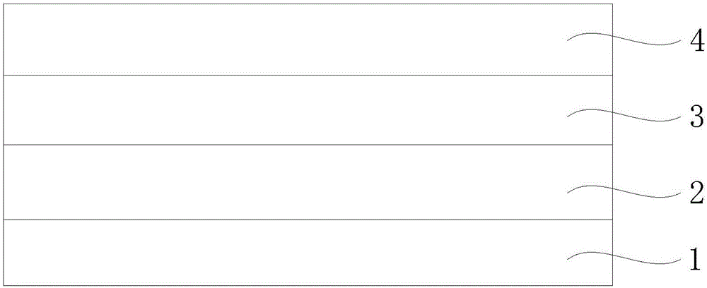
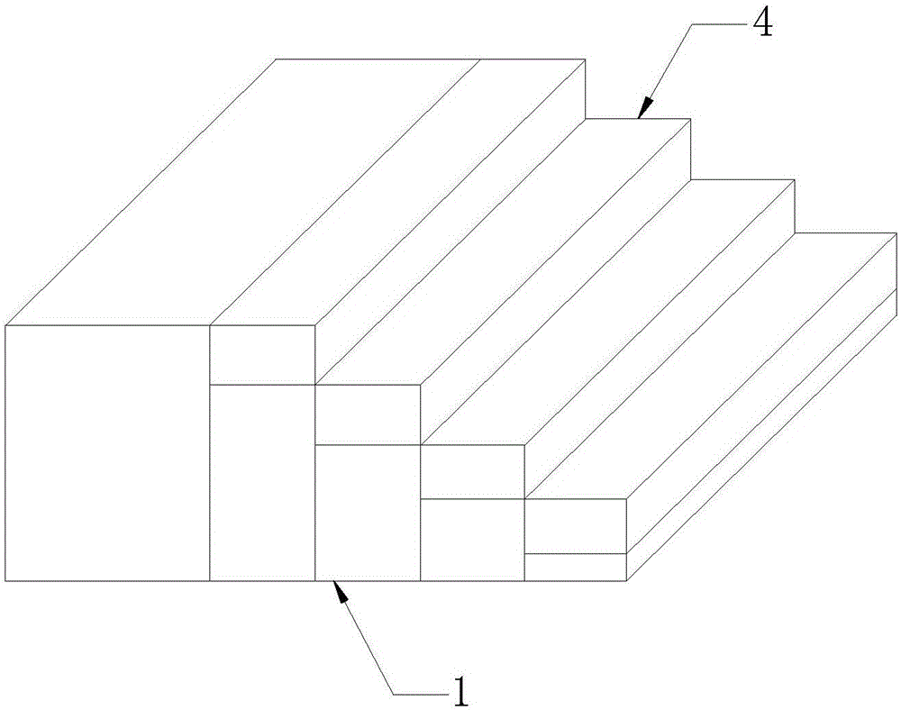
[0031] In the drawings, the thicknesses of layers and regions are exaggerated for clear illustration of components. Furthermore, the same reference numerals may be used to refer to the same elements throughout the specification and drawings.

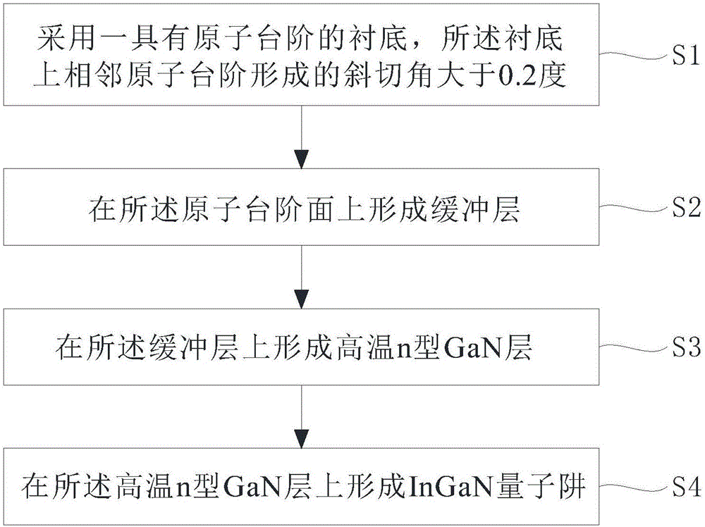
[0032] figure 1 It is a flow chart of the steps of the method for improving the l...


PUM

PropertyMeasurementUnit
Thicknessaaaaaaaaaa
Thicknessaaaaaaaaaa
Electron concentrationaaaaaaaaaa

Abstract

The invention discloses a method and a structure for improving luminous efficiency of a green light wavelength or longer wavelength InGaN quantum well. The method comprises the following steps of adopting a substrate with atomic steps, wherein a chamfer angle formed between the adjacent atomic steps on the substrate is greater than 0.2 degrees; forming a buffer layer on the atomic step surfaces; forming a high-temperature n type GaN layer on the buffer layer; and forming the InGaN quantum well on the high-temperature n type GaN layer. According to the method for improving the luminous efficiency of the InGaN quantum well by adopting the large-chamfer-angle substrate, an active region of the green light wavelength or longer wavelength InGaN quantum well is grown on the substrate with the chamfer angle greater than 0.2 degrees, so that atomic step flow growth of the green light wavelength or longer wavelength InGaN quantum well can be realized, the morphology can be improved, and the internal quantum efficiency of the InGaN quantum well can be improved. In addition, the InGaN quantum well prepared by the above method can be widely applied to a GaN-based green light wavelength or longer wavelength LED or a GaN-based green light wavelength or longer wavelength laser, and also can be widely applied to a multi-quantum-well solar cell.

Description

technical field [0001] The invention belongs to the technical field of semiconductors, and in particular relates to a method and structure for improving the luminous efficiency of green light or longer wavelength InGaN quantum wells. Background technique [0002] GaN-based green or longer wavelength lasers and LEDs are widely used in semiconductor display and lighting. The active region of InGaN quantum well is the core structure of GaN-based lasers and LEDs, and its growth behavior and morphology have a very important impact on the optical properties of InGaN quantum wells and device performance. [0003] Due to the very high equilibrium vapor pressure of InN and the weak In-N bond energy, the decomposition temperature of InN is low. Therefore, InGaN with a high In composition must be grown at a low temperature to ensure that enough In is incorporated into the epitaxial layer. Generally, the temperature for growing InGaN by MOCVD is between 650°C and 750°C. But usually a...

Claims


Application Information

Patent Timeline
IPC IPC(8): H01L33/00H01L33/20H01L33/24H01L33/32H01S5/343B82Y30/00B82Y40/00
CPCB82Y30/00B82Y40/00H01L33/0075H01L33/20H01L33/24H01L33/32H01S5/34333
Inventor 田爱琴刘建平张书明李德尧张立群杨辉
Owner SUZHOU INST OF NANO TECH & NANO BIONICS CHINESE ACEDEMY OF SCI
Learn More