Deep ultraviolet LED packaging device and preparation method thereof

A technology of LED packaging and deep ultraviolet, which is applied in the direction of electric solid-state devices, semiconductor devices, electrical components, etc., can solve problems such as aging, short service life, and complex packaging structure, so as to prevent the aging of intermediate insulating layer materials, improve reliability and The effect of service life and simple and easy preparation process

Active Publication Date: 2017-05-31
APT ELECTRONICS
View PDF6 Cites 14 Cited by
  • Summary
  • Abstract
  • Description
  • Claims
  • Application Information

AI Technical Summary

Problems solved by technology

However, in the traditional deep-ultraviolet LED packaging technology, due to certain defects in materials such as the adhesive layer, the UV light is easily absorbed by the adhesive layer, making the adhesive layer easy to turn yellow, aging, etc., which in turn leads to deep ultraviolet radiation. LED has many disadvantages such as low luminous power, poor heat dissipation, low reliability and short service life.
[0004] For example, the Chinese patent application number 201420396320.9 discloses a deep ultraviolet LED device packaging structure, including a ceramic support 1 and a deep ultraviolet chip 5 arranged on the base of the ceramic support 1. The deep ultraviolet chip 5 is connected by a silver wire 6. To the positive and negative electrodes, the ceramic support 1 is bonded with a quartz lens 2 through an adhesive material 4. This packaging structure has the following defects: (1) The adhesive material is easy to absorb UV light and cause self-aging, thereby causing the luminous power of the LED device to decrease. Low and low reliability; (2) The packaging structure is relatively complicated, the production cost is high, and the heat dissipation is poor, and the ceramic bracket and the quartz lens are connected by bonding, so the reliability is not very high
In this patent, the glass cover plate and the substrate are fastened and connected by setting a pressure ring structure, thereby avoiding the problems of easy aging of the adhesive and low reliability of the LED device due to the use of bonding, but the packaging structure is also the same. It is more complicated, the production cost is higher, and the heat dissipation is relatively poor

Method used


Image

  • Deep ultraviolet LED packaging device and preparation method thereof
  • Deep ultraviolet LED packaging device and preparation method thereof
  • Deep ultraviolet LED packaging device and preparation method thereof

Examples


Embodiment 1

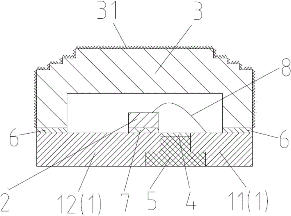
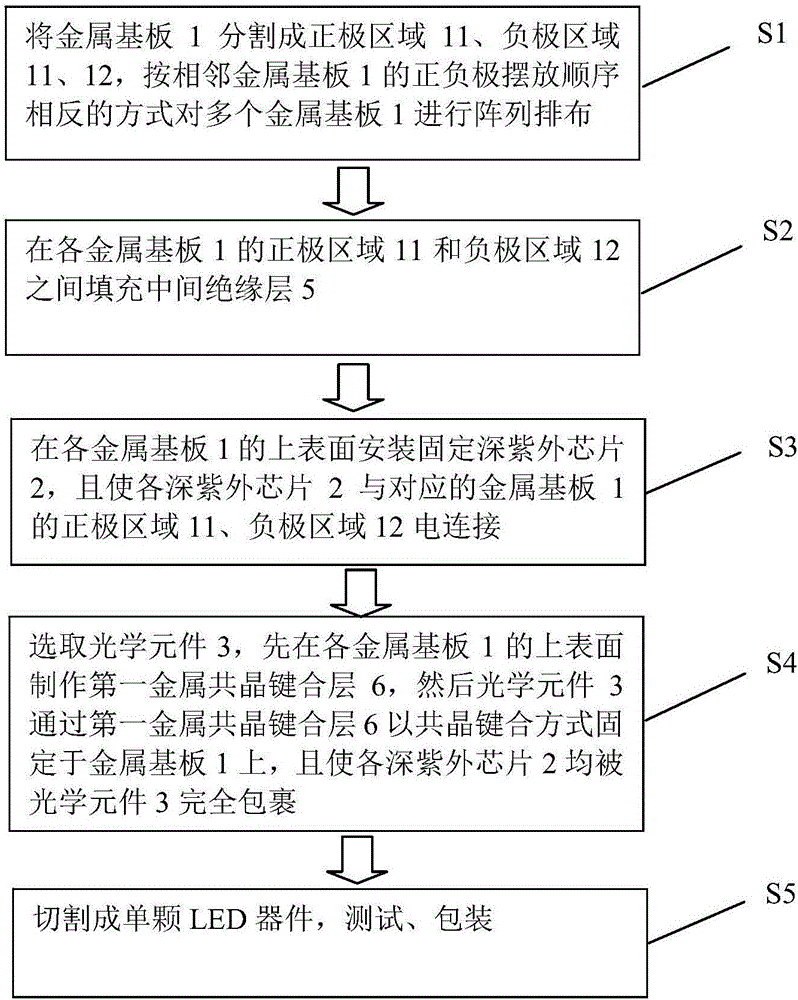
[0038] This embodiment discloses a deep ultraviolet LED packaging device, such as figure 1 As shown, it includes a metal substrate 1 , a deep ultraviolet chip 2 , an optical element 3 , an intermediate insulating layer 5 and a first metal eutectic bonding layer 6 .

[0039] Wherein, the positive electrode region 11 and the negative electrode region 12 of the metal substrate 1 are separated by the intermediate insulating layer 5; the deep ultraviolet chip 2 is fixed on the metal substrate 1, and the deep ultraviolet chip 2 is electrically connected with the positive electrode region 11 and the negative electrode region 12 of the metal substrate 1 .

[0040] Wherein, the optical element 3 is fixed on the metal substrate 1 through the first metal eutectic bonding layer 6 , and the optical element 3 completely wraps the deep ultraviolet chip 2 . In other words, in the present invention, the optical element 3 and the metal substrate 1 are combined by the metal eutectic bonding met...

Embodiment 2

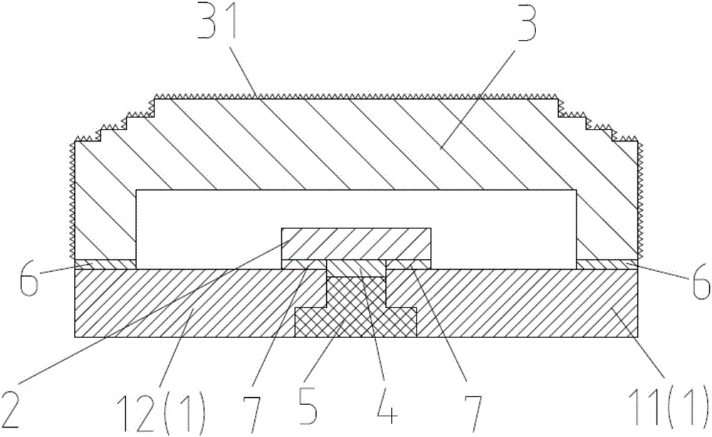
[0070] This embodiment discloses another deep-ultraviolet LED packaging device. In terms of structure, the difference between it and the deep-ultraviolet LED packaging device described in Embodiment 1 lies in:

[0071] Such as figure 2 As shown, the deep ultraviolet chip 2 is a flip chip, and the positive electrode region 11 and the negative electrode region 12 of the metal substrate 1 are provided with a second metal eutectic bonding layer 7, and the deep ultraviolet chip 2 (specifically, a flip chip) passes through the second metal eutectic bonding layer 7. The metal eutectic bonding layer 7 is electrically connected to the positive electrode region 11 and the negative electrode region 12 of the metal substrate 1 .

[0072] For the preparation method of deep ultraviolet LED packaging device, the difference between this embodiment and embodiment 1 lies in:

[0073] In step S4, the DUV chip 2 is selected as a flip chip, and the positive electrode region 11 and the negative e...


PUM


Abstract

The invention discloses a deep ultraviolet LED packaging device. The device comprises a metal substrate, a deep ultraviolet chip, an optical element, an intermediate insulating layer and a first metal eutectic bonding layer, wherein a positive electrode region and a negative electrode region of the metal substrate are separated by the intermediate insulating layer; the deep ultraviolet chip is fixed on the metal substrate and electrically connected with the positive electrode region and the negative electrode region of the metal substrate; the optical element is fixed on the metal substrate through the first metal eutectic bonding layer and completely wraps the deep ultraviolet chip; the device further comprises an SiO2 insulating layer which covers the inner surface of the intermediate insulating layer. The invention further discloses a preparation method of the deep ultraviolet LED packaging device. The deep ultraviolet LED packaging device has the advantages of high luminous power, good heat dissipation, significantly improved product reliability and significantly prolonged service life, the packaging structure is simple, and reduction of the preparation cost is facilitated; the preparation method of the deep ultraviolet LED packaging device is simple and easy in process, suitable for production line work and high in preparation efficiency.

Description

technical field [0001] The invention belongs to the technical field of deep ultraviolet LED packaging, and in particular relates to a deep ultraviolet LED packaging device and a preparation method thereof. Background technique [0002] In ultraviolet light, light with a wavelength of 200 nanometers to 350 nanometers is called deep ultraviolet light. Due to its advantages of high efficiency, environmental protection, energy saving and reliability, deep ultraviolet LED (DUVLED) has great application value in the fields of lighting, sterilization, medical treatment, printing, biochemical detection, high-density information storage and confidential communication. These advantages are Ordinary UV LEDs are unmatched. [0003] Due to the short wavelength and strong energy of deep ultraviolet LEDs, the material performance is seriously degraded, so extremely high requirements are put forward for packaging technology and packaging materials. However, in the traditional deep-ultravi...

Claims


Application Information

Patent Timeline
Patent Type & Authority Applications(China)
IPC IPC(8): H01L33/48H01L33/56H01L33/58H01L33/62H01L33/64
CPCH01L2224/16245H01L2224/48091H01L2224/48247H01L2224/73265H01L2924/00014H01L33/48H01L33/56H01L33/58H01L33/62H01L33/647H01L2933/0033H01L2933/005H01L2933/0058H01L2933/0066H01L2933/0075
Inventor 万垂铭曾照明姜志荣朱文敏李真真侯宇肖国伟
Owner APT ELECTRONICS
Why Eureka
Try Eureka