Composite quantum dot light emitting diode device and preparation method thereof
A quantum dot light-emitting and composite light-emitting layer technology, applied in the field of quantum dots, can solve the problems of low luminous efficiency and high turn-on voltage of light-emitting diodes, and achieve the effects of improving interface properties, reducing turn-on voltage, and enhancing luminous efficiency
- Summary
- Abstract
- Description
- Claims
- Application Information
AI Technical Summary
Problems solved by technology
Method used
Image
Examples
Embodiment 1
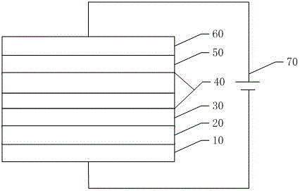
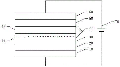
[0056] The structure of the QLED device is described as: glass substrate / ITO / PEDOT:PSS / TFB / CdSe@ZnS / CH 3 NH 3 PbBr 3 / ZnO / Al, its preparation method is as follows:
[0057] a. Spin-coat one deck of PEDOT on ITO substrate:PSS thin film is used as hole injection layer;
[0058]b. Spin-coat a TFB layer on the PEDOT:PSS layer;
[0059] c. Spin-coat a layer of CdSe@ZnS quantum dots on the TFB layer, and then spin-coat a layer of CH on the quantum dot layer 3 NH 3 PbBr 3 Organic-inorganic hybrid perovskite layer to obtain a quantum dot composite light-emitting layer;
[0060] d. Next, spin-coat a layer of ZnO on the quantum dot composite luminescent layer;
[0061] e. Finally, a layer of Al is evaporated on ZnO to obtain a quantum dot light-emitting diode device.
Embodiment 2
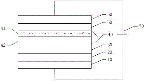
[0063] The structure of the QLED device is described as: glass substrate / ITO / PEDOT:PSS / TFB / CH 3 NH 3 PbBr 3 / CdSe@ZnS / ZnO / Al, its preparation method is as follows:
[0064] a. Spin-coat one deck of PEDOT on ITO substrate:PSS thin film is used as hole injection layer;
[0065] b. Spin-coat a TFB layer on the PEDOT:PSS layer;
[0066] c. Spin-coat a layer of CH on the TFB layer 3 NH 3 PbBr 3 Organic-inorganic hybrid perovskite layer, and then spin-coat a layer of CdSe@ZnS quantum dot layer on the organic-inorganic hybrid perovskite layer to obtain a quantum dot composite light-emitting layer;
[0067] d. Next, spin-coat a layer of ZnO on the quantum dot composite luminescent layer;
[0068] e. Finally, evaporate a layer of Al on the ZnO to obtain a quantum dot light-emitting diode.
Embodiment 3
[0070] The structure of the QLED device is described as: glass substrate / ITO / PEDOT:PSS / TFB / CH 3 NH 3 PbBr 3 &CdSe@ZnS / ZnO / Al, its preparation method is as follows:
[0071] a. Spin-coat one deck of PEDOT on ITO substrate:PSS thin film is used as hole injection layer;
[0072] b. Spin-coat a TFB layer on the PEDOT:PSS layer;
[0073] c. First combine CdSe@ZnS quantum dots with CH 3 NH 3 PbBr 3 The organic-inorganic hybrid perovskite material is mixed uniformly at a ratio of 0.1:1, dissolved in a mixed solvent of n-hexane and N,N-dimethylformamide, and then the mixed solution is spin-coated on the TFB layer to obtain Quantum dot composite luminescent layer;
[0074] d. Next, spin-coat a layer of ZnO on the quantum dot composite luminescent layer;
[0075] e. Finally, evaporate a layer of Al on the ZnO to obtain a quantum dot light-emitting diode.
PUM
| Property | Measurement | Unit |
|---|---|---|
| Thickness | aaaaa | aaaaa |
| Thickness | aaaaa | aaaaa |
Abstract
Description
Claims
Application Information


