Preparation method of GaAs-based horizontal plasma pin diode for multi-layer holographic antenna

A holographic antenna and plasma technology, applied in antennas, antenna parts, antenna supports/mounting devices, etc., can solve problems such as uneven doping concentration, large implant dose and energy, and incompatibility, and achieve enhanced controllability , easy processing, and performance-enhancing effects

Active Publication Date: 2017-06-13
潘芊璇
View PDF2 Cites 2 Cited by
  • Summary
  • Abstract
  • Description
  • Claims
  • Application Information

AI Technical Summary

Problems solved by technology

[0003] At present, the materials used in pin diodes used in plasma reconfigurable holographic antennas at home and abroad are all bulk silicon materials. This material has the problem of low carrier mobility in the intrinsic region, which affects the carrier concentration in the intrinsic region of the pin diode. In turn, it affects its solid-state plasma concentration; and the P region and N region of this structure are mostly formed by implantation process, which requi

Method used


Image

  • Preparation method of GaAs-based horizontal plasma pin diode for multi-layer holographic antenna
  • Preparation method of GaAs-based horizontal plasma pin diode for multi-layer holographic antenna
  • Preparation method of GaAs-based horizontal plasma pin diode for multi-layer holographic antenna

Examples


Embodiment 1

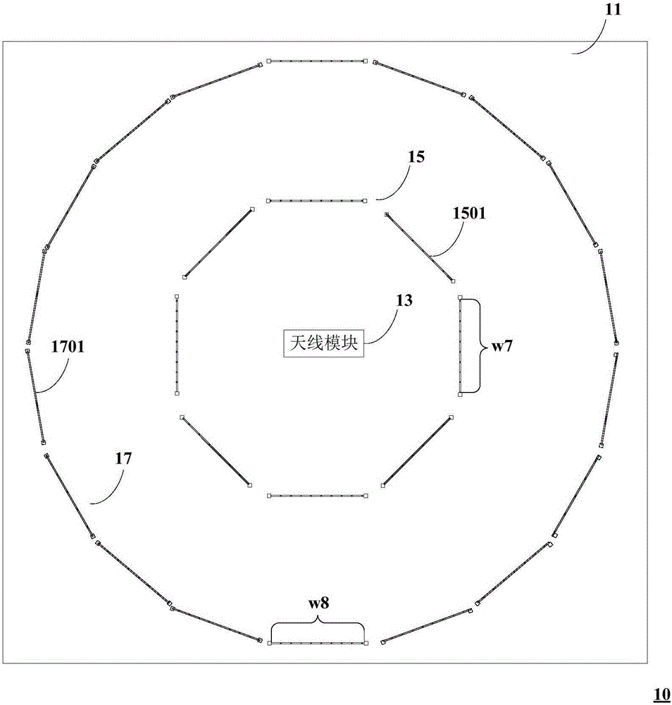
[0054]The embodiment of the present invention proposes a method for preparing a GaAs-based lateral plasmonic pin diode for a multilayer holographic antenna, and the GaAs-based plasmonic pin diode is used for making a reconfigurable holographic antenna. See figure 1 , figure 1 It is a structural diagram of a multi-layer reconfigurable holographic antenna according to an embodiment of the present invention. The multi-layer holographic antenna includes: a semiconductor substrate GeOI, an antenna module, a first holographic ring and a second holographic ring; wherein, the The antenna module, the first holographic ring and the second holographic ring all include GaAs-based plasma pin diode strings connected in series; the GaAs-based plasma pin diode strings include a plurality of serially connected GaAs-based plasma pin diode strings. pin diode.

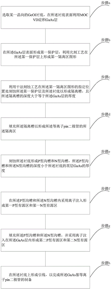
[0055] See image 3 , image 3 It is a flowchart of a method for manufacturing a GaAs-based lateral plasmonic pin diode according to...

Embodiment 2

[0098] See Figure 4a-Figure 4s , Figure 4a-Figure 4s It is a schematic diagram of a method for preparing a Ge-based plasma pin diode according to an embodiment of the present invention. On the basis of the first embodiment above, to prepare a Ge-based solid-state plasma pin diode with a channel length of 22nm (the length of the solid-state plasma region is 100 microns) As an example to describe in detail, the specific steps are as follows:

[0099] Step 1, substrate material preparation steps:

[0100] (1a) if Figure 4a As shown, a GeOI substrate 101 with (100) crystal orientation is selected, and a GaAs layer 102 is deposited on the top layer Ge by MOCVD method, the doping type is p-type, the doping concentration is 1014cm-3, and the thickness of the top layer GaAs is 50 μm ;

[0101] (1b) if Figure 4b As shown, a first SiO2 layer 201 with a thickness of 40nm is deposited on GaAs by chemical vapor deposition (Chemical vapor deposition, CVD for short);

[0102] (1c) ...

Embodiment 3

[0131] Please refer to Figure 5 , Figure 5 It is a schematic diagram of a device structure of a Ge-based plasmonic pin diode according to an embodiment of the present invention. The plasmonic pin diode employs the above as figure 1 The preparation method shown is made, specifically, the plasma pin diode is prepared and formed on the GeOI substrate 301, and the P region 305, the N region 306 of the pin diode and the laterally located between the P region 305 and the N region 306 I regions are located in the top layer of the substrate GaAs302. Wherein, the pin diode can be isolated by STI deep trenches, that is, an isolation trench 303 is provided outside the P region 305 and the N region 306, and the depth of the isolation trench 303 is greater than or equal to the thickness of the top Ge layer. In addition, the P region 305 and the N region 306 may respectively include a thin-layer P-type active region 307 and a thin-layer N-type active region 304 along the substrate dire...


PUM


Abstract

The invention relates to a preparation method of a GaAs-based horizontal plasma pin diode for a multi-layer holographic antenna. The multi-layer holographic antenna comprises a semiconductor substrate GeOI, an antenna module, a first holographic round ring and a second holographic round ring, wherein the antenna module, the first holographic round ring and the second holographic round ring all comprises GaAs-based plasma pin diodes which are sequentially connected in series. The preparation method of the GaAs-based plasma pin diode comprises the steps of selecting a GeOI substrate in a certain crystal direction, depositing a GaAs layer on a surface of the substrate and forming an isolation region by metal-organic chemical vapor deposition (MOCVD); etching the substrate to form a P-type groove and an N-type groove and form a first P-type active region and a first N-type active region; and filling the P-type groove and N-type groove, forming a lead on the substrate to complete the preparation of the GaAs-based plasma pin diode. According to the embodiment, the high-performance GaAs-based plasma pin diode can be prepared and provided for forming the multi-layer holographic antenna by a deep groove isolation technology and an ion injection process.

Description

technical field [0001] The invention relates to the technical field of semiconductor device manufacturing, in particular to a method for preparing a GaAs-based lateral plasma pin diode used for a multilayer holographic antenna. Background technique [0002] The holographic antenna consists of a source antenna and a holographic structure. Combined with actual needs, select an appropriate antenna as the source antenna, change the radiation of the feed source by loading a holographic structure to obtain the required radiation characteristics of the target antenna, and calculate the antenna structure through the given interference pattern of electromagnetic wave radiation. Compared with the traditional reflector antenna, the holographic structure has a flexible construction form, which is convenient for integrated design with the application environment, and has a wide range of applications. [0003] At present, the materials used in pin diodes used in plasma reconfigurable hol...

Claims


Application Information

Patent Timeline
IPC IPC(8): H01L21/329H01L29/868H01L29/20H01Q1/22H01Q1/36
CPCH01L29/20H01L29/6609H01L29/868H01Q1/2283H01Q1/36
Inventor 尹晓雪张亮
Owner 潘芊璇
Why Eureka
Try Eureka