

Silicon carbide semiconductor device and preparation method therefor
A semiconductor and silicon carbide technology, applied in the field of silicon carbide semiconductor devices, can solve the problems of limiting the application of SiCIGBT devices and high voltage drop in the drift region, achieve good conduction characteristics and switching characteristics, improve device conduction performance, and improve emitter injection than the effect
- Summary
- Abstract
- Description
- Claims
- Application Information
AI Technical Summary
Problems solved by technology
Method used
Image

Examples
Embodiment Construction
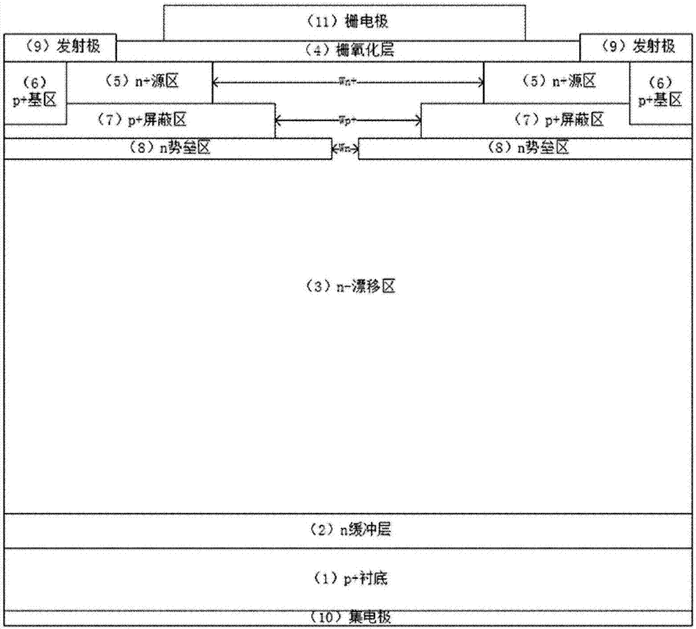
[0046] In the present invention, the directional terms such as "upper", "lower", "adjacent", "below" or "above" only refer to the directions of the attached drawings, wherein "upper", "lower", " Under" or "over" means contact or non-contact with a single or multiple elements. These directional terms are used to illustrate, not to limit the invention.
[0047] In order to reduce the high drift region resistance of the silicon carbide IGBT device, reduce the conduction voltage drop of the device, and improve the conduction capability of the silicon carbide IGBT device. The invention provides a silicon carbide device structure, which can be applied to high-voltage conditions such as traction transmission and smart grids. In addition, the device can also greatly increase the carrier concentration in the drift region during the conduction process of the device, so that the conduction of the device It has an extremely low drift region on-resistance when on.
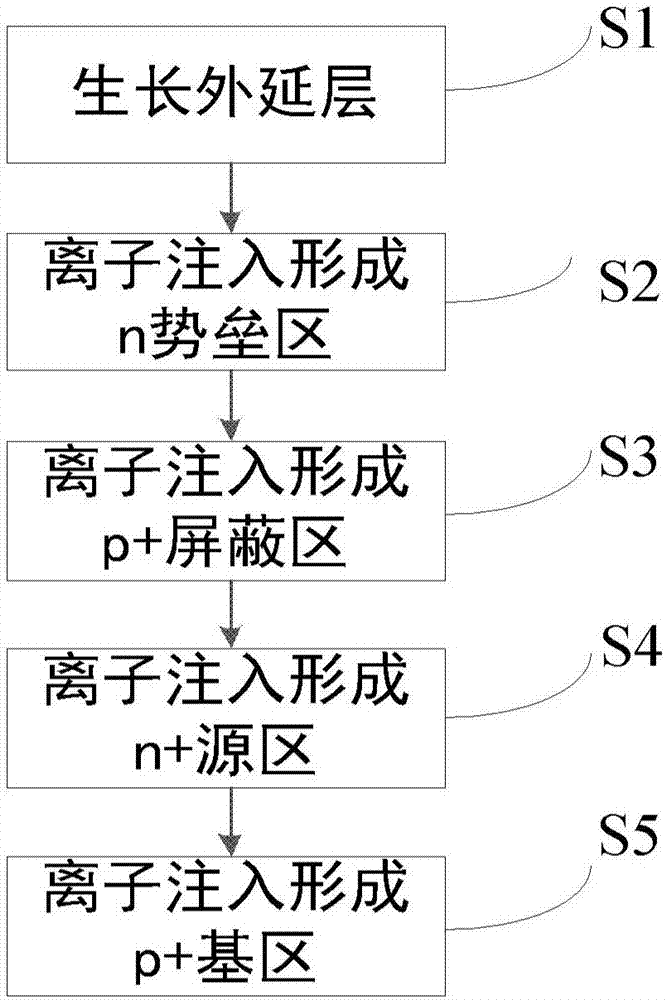
[0048] In order to ma...
PUM
 Abstract
Description
Claims
Application Information