Power device with fixed interface charge field limitation ring

A technology of interface charge and power devices, which is applied in the direction of electrical components, semiconductor devices, circuits, etc., can solve problems such as breakdown voltage drop and device failure, and achieve the goals of reducing device size, improving integration, and increasing output current and power density Effect

Active Publication Date: 2017-06-20
GUILIN UNIV OF ELECTRONIC TECH +1
View PDF3 Cites 2 Cited by
  • Summary
  • Abstract
  • Description
  • Claims
  • Application Information

AI Technical Summary

Problems solved by technology

[0005] The technical problem to be solved by the present invention is the breakdown voltage drop and device failure caused by impurity d

Method used


Image

  • Power device with fixed interface charge field limitation ring
  • Power device with fixed interface charge field limitation ring
  • Power device with fixed interface charge field limitation ring

Examples


Embodiment 1

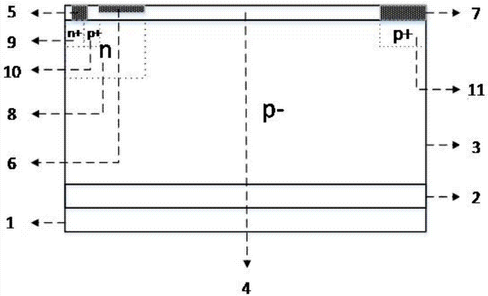
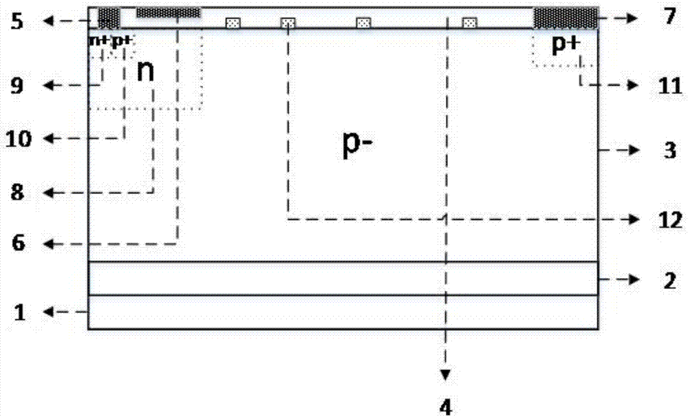
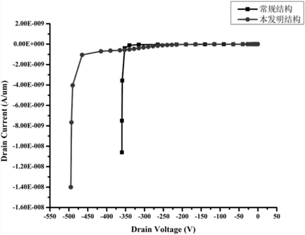
[0031] A power device with a fixed interfacial charge field limiting ring is a P-type SOI LDMOS device, such as figure 2 As shown, including substrate 1, buried layer 2, P - Drift region 3, field oxygen layer 4, source electrode 5, gate electrode 6, drain electrode 7, N well 8, N well + Contact zone 9, P + Source region 10, P + Drain region 11 and at least one fixed interface charge region 12 .

[0032] Substrate 1, buried layer 2, P - The drift region 3 and the field oxygen layer 4 are stacked sequentially from bottom to top. where P - The drift region 3 is the active layer. The source electrode 5 , the gate electrode 6 and the drain electrode 7 are arranged on both sides of the field oxygen layer 4 , wherein the source electrode 5 and the gate electrode 6 are located on the left side of the field oxygen layer 4 , and the drain electrode 7 is located on the right side of the field oxygen layer 4 . N well 8, N + Contact zone 9, P + Source region 10, P + The drain re...

Embodiment 2

[0040] Another power device with a fixed interfacial charge field limiting ring is a power diode, such as Figure 6 As shown, including substrate 1, N - Drift region 13, field oxygen layer 4, anode P + Zone 14, Cathode N + zone 15, anode 16, cathode 17, and at least one fixed interface charge zone 12.

[0041] Substrate 1, N - The drift region 13 and the field oxygen layer 4 are stacked sequentially from bottom to top. where N - The drift region 13 is the active layer. Anode P + Zone 14 and Cathode N + District 15 is located in N - upper part of the drift region 13, and with N - The upper surface of the drift region 13 is in contact. The anode 16 and the cathode 17 are arranged on both sides of the field oxygen layer 4 , wherein the anode 16 is located on the left side of the field oxygen layer 4 , and the cathode 17 is located on the right side of the field oxygen layer 4 .

[0042] The fixed interface charge region 12 is located at the lower part of the field oxyg...


PUM

PropertyMeasurementUnit
Heightaaaaaaaaaa

Abstract

The invention discloses a power device with a fixed interface charge field limitation ring. The power device comprises a field oxide layer and an active layer, wherein the field oxide layer is arranged on the active layer, at least one fixed interface charge region is arranged in the field oxide layer, and the fixed interface charge region is arranged at a lower part of the field oxide layer and is in contact with a lower surface of the field oxide layer, namely an interface surface of the field oxide layer and the active layer. By the power device, the problems of breakdown voltage drop and device failure caused by impurity diffusion in an FLR region of an existing power device can be solved, the breakdown voltage of the device is effectively improved, the electric field distribution of a surface of the active layer is improved, and the electric field distribution is more uniform.

Description

technical field [0001] The invention relates to the technical field of semiconductor power devices, in particular to a power device with a fixed interface charge field limiting ring. Background technique [0002] Power integrated circuit (Power Integrated Circuit, PIC) integrates signal processing, sensing protection, and power transmission technology. It has developed rapidly since it was produced in the 1980s. High-tech industry has a very wide range of applications. PIC is an important branch of integrated circuits. Compared with discrete devices, PIC not only has great advantages in performance, power consumption and stability, but also has great significance for reducing cost, volume and weight. Therefore, experts and scholars at home and abroad have devoted great attention and in-depth research to PIC. [0003] Power semiconductor devices mainly include power diodes, thyristors, power MOSFETs, power insulated gate bipolar transistors (IGBTs) and wide bandgap power se...

Claims


Application Information

Patent Timeline
IPC IPC(8): H01L29/06
CPCH01L29/0611H01L29/0684
Inventor 李琦文艺李海鸥首照宇陈永和杨年炯李思敏张法碧高喜傅涛
Owner GUILIN UNIV OF ELECTRONIC TECH
Why Eureka
Try Eureka