Additive-assisted perovskite solar cell and preparation method thereof
A solar cell and perovskite technology, applied in circuits, photovoltaic power generation, electrical components, etc., can solve the problems of low device efficiency, high heating temperature, and long time consumption, so as to improve efficiency and stability, and increase steady-state output power , Eliminate the effect of positive and negative scanning differences
- Summary
- Abstract
- Description
- Claims
- Application Information
AI Technical Summary
Problems solved by technology
Method used
Image
Examples
preparation example Construction
[0045] The preparation of the above-mentioned perovskite solar cell comprises the following steps:
[0046] A) preparing a bottom charge collection layer on the bottom electrode layer;
[0047] B) Preparation of organic-inorganic perovskite active light-absorbing layer on the bottom charge collection layer by additive-assisted growth method, or deposition on the substrate consisting of bottom electrode / bottom charge collection layer / top electrode layer modified with / without top charge collection layer Perovskite active light-absorbing layer, thus completing the battery preparation;
[0048] C) For the case where the perovskite active light-absorbing layer is prepared directly on the bottom charge collection layer, the top charge collection layer and the top electrode layer are sequentially prepared on the surface of the organic-inorganic perovskite active light-absorbing layer to complete the preparation of the battery device.
[0049] Wherein, the preparation methods of the ...
Embodiment 1
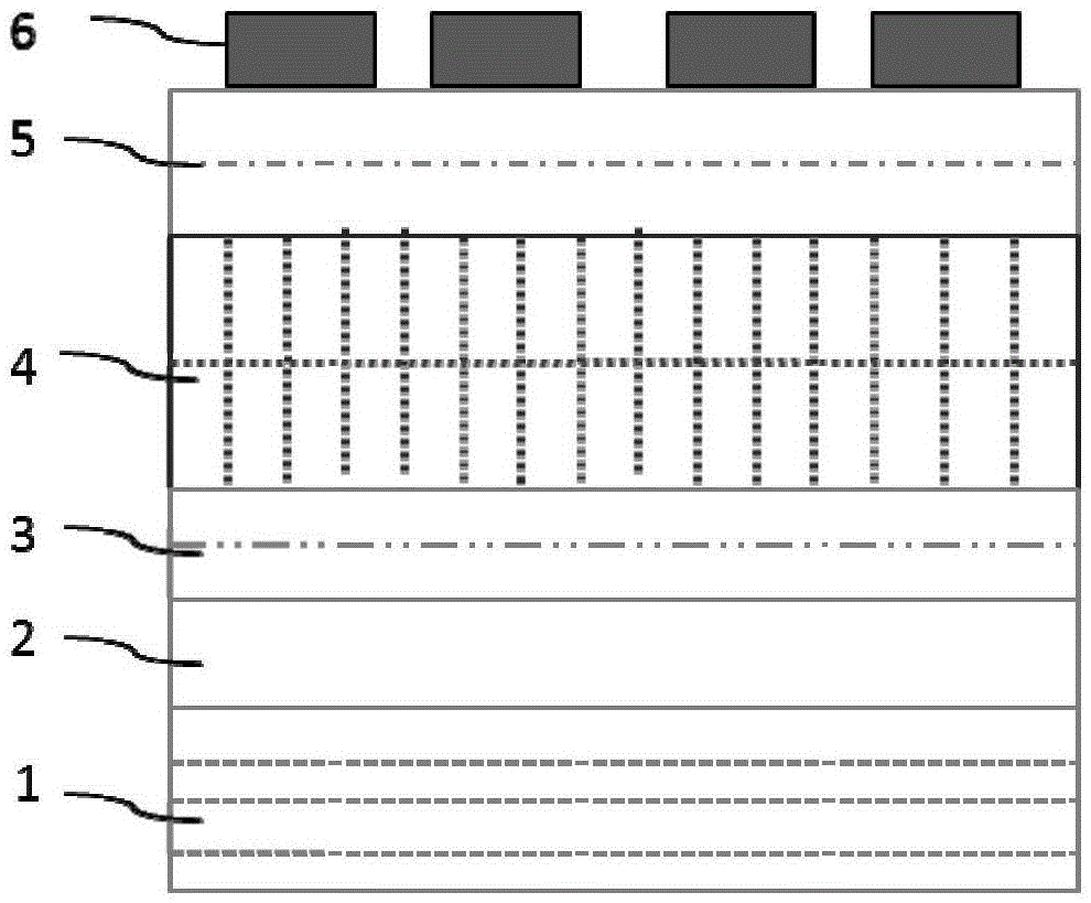
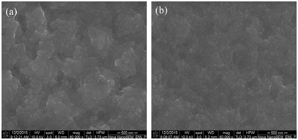
[0069] Using glass as the substrate, deposit a transparent and conductive ITO layer on the surface of the glass plate, deposit PEDOT:PSS with a certain thickness such as 40nm on the surface of the ITO transparent electrode layer as the hole transport layer, and heat at 130°C for 20 minutes. 1mmol of Pb(Ac) 2 and 3mmol of MAI were dissolved in 1ml of DMF to prepare Pb(Ac) 2 :MAI mixed solution, this mixed solution is spin-coated on the conductive substrate ITO that has prepared PEDOT:PSS layer modification, and is heated at a certain temperature (such as 80 ℃) 5-10min, obtains CH 3 NH 3 PB 3 Perovskite active layer, the SEM test results of this film are as follows image 3 shown. The obtained films have high coverage and clear crystal grains. However, the flatness of the film surface is not good. followed by figure 2 As shown in the process, complete figure 1 The cells shown were fabricated at a standard solar intensity (AM1.5, 100mW / cm 2 ) under the irradiation of th...
Embodiment 2
[0073] Configure Pb(Ac) 2 : DMF solution of MAI (molar ratio 1:2.95~3.05), mix 0.1-0.5mol / L MABr additive into Pb(Ac) in volume ratio 1:100 (the solvent used for the additive is DMF) 2 : In the MAI solution, the MABr concentration obtained is Pb(Ac) 2 0.5-2mol% mixed perovskite solution. The mixed solution is spin-coated on the ITO transparent conductive bottom electrode layer modified by PEDOT:PSS, and heated at a certain temperature (such as 80°C) for 5-10min, and sintered into CH 3 NH 3 PB 3 The perovskite active layer, the SEM test results of the surface morphology of the active layer are as follows image 3 shown. From the comparison of the SEM surface morphology, it can be seen that after the addition of MABr additives, a smoother perovskite film was obtained. Such as figure 2 complete as shown figure 1 structure of solar cells, at a standard solar intensity (AM1.5, 100mW / cm 2 ) irradiation, test battery performance, the best device performance statistics are s...
PUM
 Abstract
Description
Claims
Application Information


