Manufacturing method of groove type super junction

A manufacturing method and super-junction technology, applied in semiconductor/solid-state device manufacturing, electrical components, circuits, etc., to achieve the effects of increasing doping concentration, reducing process difficulty, and reducing forward conduction resistance

Inactive Publication Date: 2017-08-15
SHANGHAI HUAHONG GRACE SEMICON MFG CORP
View PDF3 Cites 2 Cited by
  • Summary
  • Abstract
  • Description
  • Claims
  • Application Information

AI Technical Summary

Problems solved by technology

However, under the current process plan, it is necessary to reduce the pitch, which is completely dependent on the optimization of the trench etching process; thus, the trench etching process has become a major bottleneck in the development of the entire process.

Method used


Image

  • Manufacturing method of groove type super junction
  • Manufacturing method of groove type super junction
  • Manufacturing method of groove type super junction

Examples


Embodiment Construction

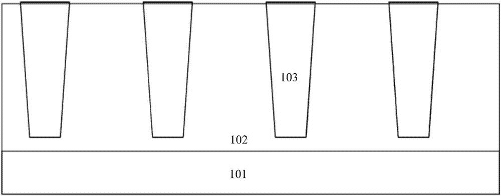
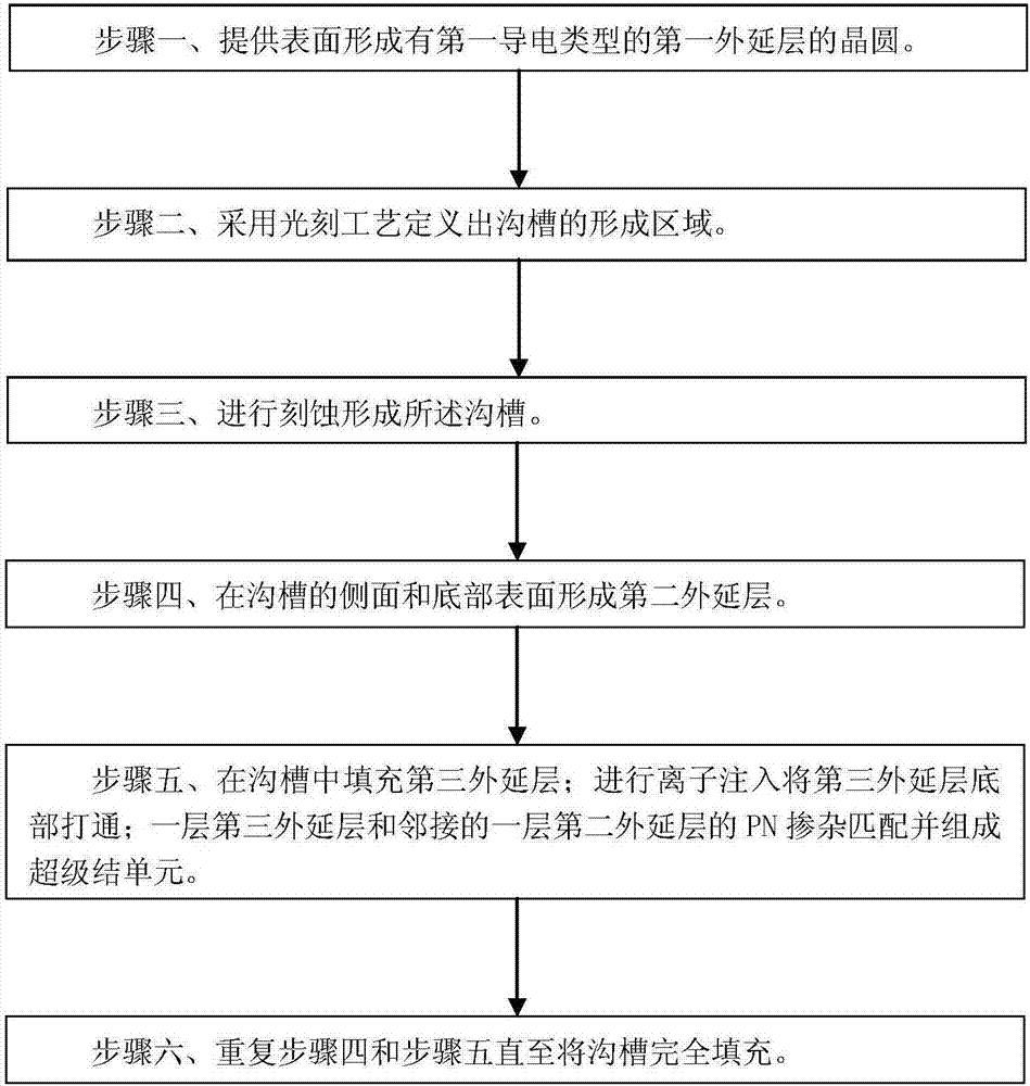
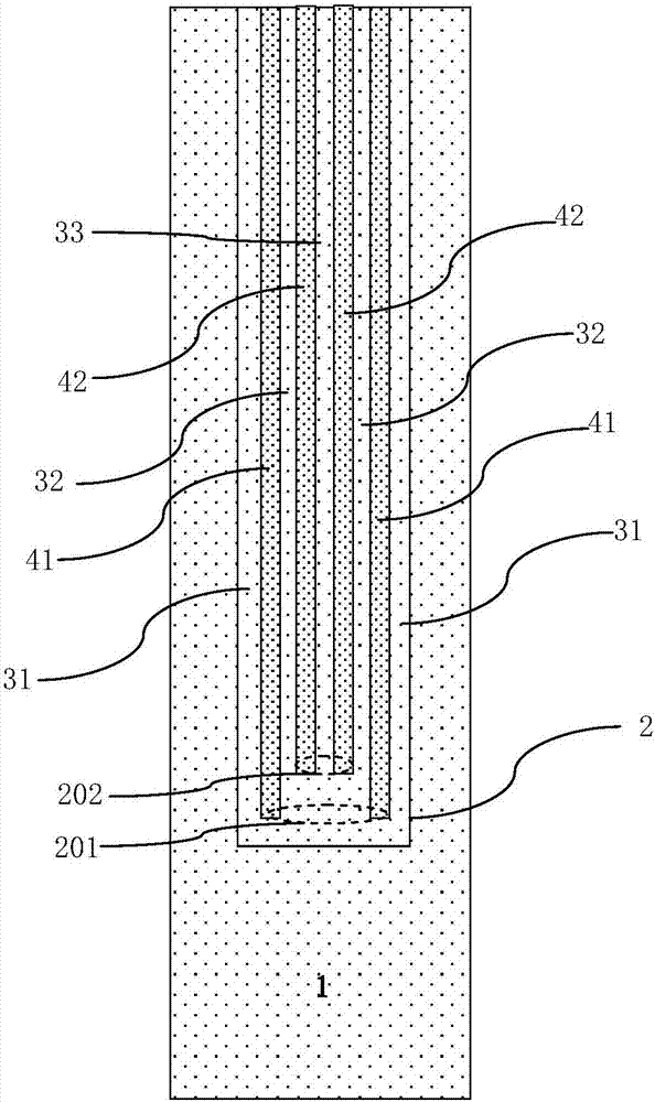
[0039] Such as figure 2 Shown is a flowchart of a method for manufacturing a Trench 2-type super junction according to an embodiment of the present invention; image 3 Shown is a schematic structural view of the super junction unit formed by the method of the embodiment of the present invention; the manufacturing method of the trench type 2 super junction in the embodiment of the present invention includes the following steps:

[0040] Step 1. A semiconductor substrate wafer is provided, and a first epitaxial layer 1 having a first conductivity type is formed on the surface of the semiconductor substrate wafer.

[0041] Preferably, the semiconductor substrate wafer is a silicon substrate wafer, the first epitaxial layer 1 is a silicon epitaxial layer, and the subsequently formed second epitaxial layers 31, 32 and 33 are all silicon epitaxial layers, and the third epitaxial layer 1 is a silicon epitaxial layer. Both epitaxial layers 41 and 42 are silicon epitaxial layers.

[0...


PUM

PropertyMeasurementUnit
thicknessaaaaaaaaaa
thicknessaaaaaaaaaa
thicknessaaaaaaaaaa

Abstract

The invention discloses a manufacturing method of a groove type super junction. The manufacturing method comprises the steps of: providing a wafer, wherein a first conduction type epitaxial layer is formed on the surface of the wafer; using a photolithography technique to define a groove forming region; carrying out etching to form a groove; forming second epitaxial layers on the side surfaces and the bottom part surface of the groove; filling third epitaxial layers in the groove; carrying out ion injection to get through the bottom part of the third epitaxial layer; carrying out PN doped matching of one layer of the third epitaxial layer and the adjacent one layer of the second epitaxial layer, and forming a super junction unit; and repeating the formation steps of the second epitaxial layers and the third epitaxial layers until the groove is completely filled up. The manufacturing method can reduce the stepping of the super junction unit, improve the in-surface evenness of PN doped matching of the super junction units on the same wafer, can improve the in-surface evenness of reverse breakdown voltage of the super junction device and improve the breakdown unit of the device, and can reduce the forward on resistance of the device.

Description

technical field [0001] The invention relates to a manufacturing process method of a semiconductor integrated circuit, in particular to a manufacturing method of a trench type super junction. Background technique [0002] The super junction is composed of alternately arranged P-type thin layers and N-type thin layers formed in a semiconductor substrate, using P-type thin layers, namely P-pillars (P-pillars) and N-type thin layers, namely N-type pillars (N-type pillars) -Pillar) completes the depletion layer formed by matching to support the reverse withstand voltage. The product with a super junction is a technology that uses PN charge balance to reduce the surface electric field (Resurf) in the body to improve the reverse breakdown BV of the device while maintaining A device structure with a smaller on-resistance, such as a MOSFET structure. The Pillar structure with PN interval is the biggest feature of the super junction. At present, there are two main methods for making...

Claims


Application Information

Patent Timeline
Patent Type & Authority Applications(China)
IPC IPC(8): H01L21/02H01L29/06
CPCH01L29/0634H01L21/02381H01L21/02532
Inventor 李昊
Owner SHANGHAI HUAHONG GRACE SEMICON MFG CORP
Why Eureka
Try Eureka