Method for preparing high-density electronic-grade semiconductor-purity super-long horizontal nanotube array

A nanotube array and semiconductor technology, which is applied in the direction of carbon nanotubes, nanocarbon, nanotechnology, etc., can solve the problems that the density cannot reach high current output carbon-based electronic devices, and there is a big gap in the purity of electronic grades, etc., to achieve broad commercial The effect of application prospects

Active Publication Date: 2017-08-22
TSINGHUA UNIV
View PDF2 Cites 2 Cited by
  • Summary
  • Abstract
  • Description
  • Claims
  • Application Information

AI Technical Summary

Problems solved by technology

[0008] However, the key problem restricting its current development is that the highest semiconductor purity of ultra-long horizontal carbon nanotube arrays is only 92%, which is still far from electronic-grade purity (99.9999%), and the density cannot reach high current output carbon Ideal indicators for base electronic devices

Method used


Image

  • Method for preparing high-density electronic-grade semiconductor-purity super-long horizontal nanotube array
  • Method for preparing high-density electronic-grade semiconductor-purity super-long horizontal nanotube array
  • Method for preparing high-density electronic-grade semiconductor-purity super-long horizontal nanotube array

Examples


Embodiment 1

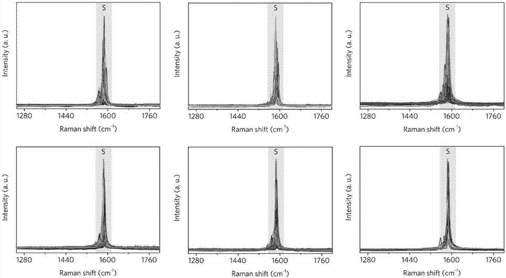
[0059] Example 1: Preparation and characterization of electronic-grade pure semiconducting ultra-long horizontal carbon nanotube arrays

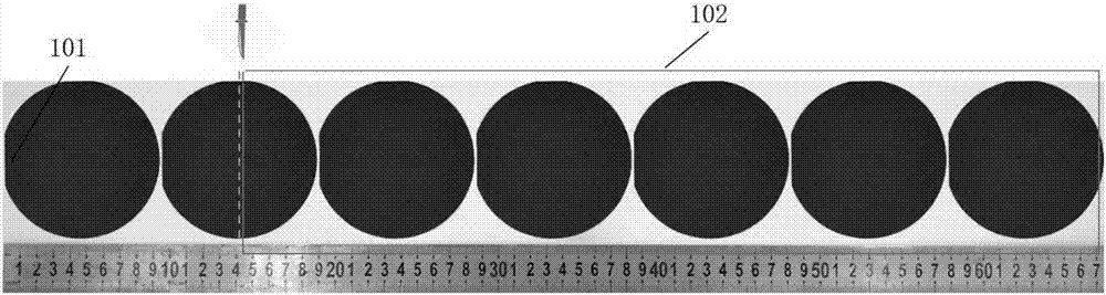
[0060] (1) Seven pieces of Si / SiO with a diameter of 10 cm are placed continuously in a cube-shaped quartz reactor 2 Wafer, with a total length of 70cm, such as figure 1 As shown, 0.05mol / L FeCl 3 Ethanol solution imprinted on the first Si / SiO 2 base front end (101);

[0061] (2) In the reactor, pass into the mixed gas (Ar:H of the argon gas of 220sccm) and hydrogen 2 =1:2, v / v) as a protective gas, and start to heat up. When the temperature rises to 1010°C, keep the temperature constant for 20min, then enter the reaction stage, and feed 160sccm methane and hydrogen gas mixture (H 2 :CH 4 =2.1:1, v / v), the reaction time continues to enter cooling stage after 30min; 2 =1:2, v / v), to prevent the carbon tube from being ablated during the cooling process;

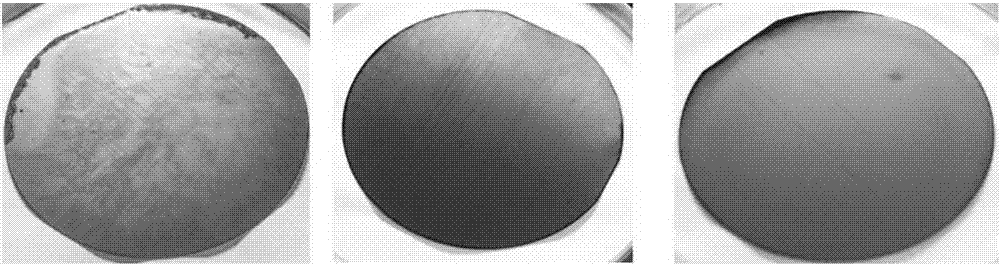
[0062] (3) When the temperature drops to room temperature, remove all Si / SiO 2 wa...

Embodiment 2

[0071]Example 2: Repeated growth improves the array density of electronic-grade purity semiconducting ultra-long horizontal carbon nanotubes

[0072] (1) Spread 0.3g FeCl upstream of the cube-shaped reactor airflow 3 Catalyst powder, feed the mixed gas of the argon of 200sccm and hydrogen (Ar:H in the reactor 2 =1:2, v / v) as a protective gas, and start to heat up, when the temperature rises to 1000°C, enter the cooling stage after constant temperature for 20min, and open the reactor when it drops to room temperature;

[0073] (2) 6 pieces of Si / SiO with a size of 5×8cm are placed continuously in the reactor 2 substrate, the growth direction of carbon nanotubes is along the width direction of the substrate, and 0.03mol / L FeCl 3 Ethanol solution imprinted on the first Si / SiO 2 basal front;

[0074] (3) Into the reactor, a mixture of argon and hydrogen of 200 sccm (Ar:H 2 =1:2, v / v) as a protective gas, and start to heat up. When the temperature rises to 1000°C, keep the tem...


PUM

PropertyMeasurementUnit
lengthaaaaaaaaaa
diameteraaaaaaaaaa
purityaaaaaaaaaa

Abstract

The invention provides a method for preparing a high-density electronic-grade semiconductor-purity super-long horizontal nanotube array. The method includes the steps that a catalyst is supported and placed on a substrate, super-long carbon nanotubes are prepared through the temperature-rise reaction, and then repeated growth, sampling, cutting and the like are conducted in sequence. In the method, through fine optimization of the carbon nanotube preparation technology and length, the high-density ultra-high-semiconductor-purity horizontal carbon nanotube array can be obtained. The simple and reliable method is provided to solve problem of the high-semiconductor-purity horizontal array carbon nanotube preparation which is a key factor restricting the development of current carbon-based integrated circuits, and has a wide commercial application prospect.

Description

technical field [0001] The invention relates to the field of preparation and application of nanomaterials, in particular, to a method for preparing a high-density electronic-grade purity semiconductor ultra-long horizontal nanotube array, so as to provide a high-purity semiconductor that is the core of the development of current carbon-based integrated circuits. The problem of preparing carbon nanotubes provides a simple and reliable technical route. Background technique [0002] Reducing chip size and improving chip performance are key manifestations of the correctness of "Moore's Law" that has driven the development of the computer industry for decades. Moore's Law, the new chip-making technology that upgrades every two years, has helped put computers on our desks, in our pockets and on our wrists. However, in the process of shrinking electronic components to the atomic scale, they are facing severe engineering challenges, resulting in the failure of the silicon-based "Mo...

Claims


Application Information

Patent Timeline
Patent Type & Authority Applications(China)
IPC IPC(8): C01B32/159C01B32/162B82Y30/00B82Y40/00
Inventor 朱振兴魏飞孙斯磊
Owner TSINGHUA UNIV
Why Eureka
Try Eureka