Laminated molybdenum disulfide field effect transistor, preparation method and application thereof

A technology of field effect transistors and molybdenum disulfide, applied in transistors, measuring devices, instruments, etc., can solve problems such as difficult to meet low voltage, complicated operation, easy to change device interface structure, etc., and achieve the effect of low turn-on voltage

Inactive Publication Date: 2017-09-29
THE NAT CENT FOR NANOSCI & TECH NCNST OF CHINA
View PDF2 Cites 7 Cited by
  • Summary
  • Abstract
  • Description
  • Claims
  • Application Information

AI Technical Summary

Problems solved by technology

However, the above-mentioned technology is obviously very limited. First, annealing and doping can easily change the interface structure of the device, which is likely to reduce the performance of field-effect devices. This makes the ability to control the turn-on voltage weak. In this article, it can only be adjusted to -20V, but it is still difficult to meet the needs of low voltage in practical applications.

Method used


Image

  • Laminated molybdenum disulfide field effect transistor, preparation method and application thereof
  • Laminated molybdenum disulfide field effect transistor, preparation method and application thereof
  • Laminated molybdenum disulfide field effect transistor, preparation method and application thereof

Examples


Embodiment 1

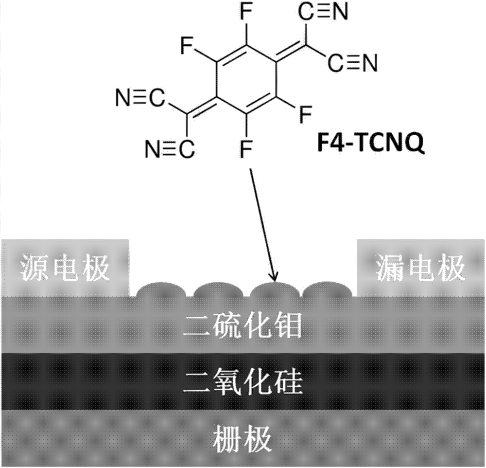
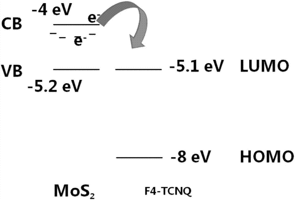
[0044] on SiO by mechanical exfoliation 2 / Si substrate to obtain MoS 2 , using electron beam exposure to prepare electrode patterns. at 3×10 -5 Vacuum deposition of 40nm / 8nm Au / Cr at a speed of 0.01nm / s in the case of Pa to obtain MoS 2 field effect transistor. Then in MoS 2 FETs, at 3 x 10 -5 Vacuum deposition of 10nm F4-TCNQ at a speed of 0.1nm / s under Pa vacuum, such as figure 2 shown. Devices were measured in a vacuum probe station, and the transfer curves were as Figure 4 shown. It can be seen that the undoped MoS 2 The turn-on voltage of the field effect transistor is -60V, and the turn-on voltage after doping F4-TCNQ is greatly reduced, about -5V. And doping F4-TCNQ reduces the sub-threshold swing of the device from 2.14V / decade to 0.91V / decade, and improves the turn-on speed of the device.

Embodiment 2

[0046] Further carried out NH 3 For the measurement of the sensor, a certain amount of NH is introduced into the vacuum chamber of the probe station 3 , to measure the sensitivity of the sensor as Figure 5 shown. It can be seen that the MoS prepared by this scheme 2 Field effect transistors can be used as NH with low gate voltage (-5V) 3 sensor, its 1000ppm sensitivity reaches about 670000%, which is much higher than the 60% sensitivity reported in the prior art (such as Late, D.J. et al.Sensing Behavior of Atomically Thin-Layered MoS 2 Transistors.ACS Nano, Volume 7, Issue 6, Pages 4879-4891), proves that the present invention has the potential application value of preparing excellent sensors.


PUM

PropertyMeasurementUnit
thicknessaaaaaaaaaa
thicknessaaaaaaaaaa

Abstract

The invention provides a laminated molybdenum disulfide field effect transistor, a preparation method and application thereof. In the laminated molybdenum disulfide field effect transistor, the surface of laminated molybdenum disulfide is covered with an F4-TCNQ molecular layer. The molybdenum disulfide is covered with small organic molecules F4-TCNQ, the molybdenum disulfide is automatically injected into the F4-TCNQ through sulfur vacancy self-doped electrons, the electron concentration in the molybdenum disulfide is reduced, and the purpose of reducing the threshold voltage of the molybdenum disulfide field effect transistor is reached. The function of an NH3 sensor under low gate voltage can be realized by using the molybdenum disulfide field effect transistor provided by the invention.

Description

technical field [0001] The invention relates to the technical field of electronic devices, in particular to a layered molybdenum disulfide field effect transistor and its preparation method and application. Background technique [0002] Two-dimensional materials such as graphene have high mobility (more than 15000cm 2 / V·s), high carrier concentration (up to 10 13 / cm 2 ), good mechanical properties, high transparency (visible band ≈ 97.7%) and other excellent characteristics, it is considered to be the next generation semiconductor material and has attracted widespread attention. However, graphene does not have a band gap, so its field-effect transistor switching ratio is low, which limits its application in electronic devices. [0003] layered molybdenum disulfide (MoS 2 ) two-dimensional semiconductor material, its single-layer energy band structure is a direct band gap with a band gap of 1.8eV, while the multi-layer energy band is an indirect band gap with a band gap...

Claims


Application Information

Patent Timeline
Patent Type & Authority Applications(China)
IPC IPC(8): H01L29/786G01N27/414
CPCH01L29/786G01N27/4141
Inventor 江潮董骥王嘉玮刘风景
Owner THE NAT CENT FOR NANOSCI & TECH NCNST OF CHINA
Why Eureka
Try Eureka