Al-doped gallium oxide X-ray detector and preparation method thereof
A gallium oxide and detector technology, applied in the field of semiconductor optoelectronic devices, can solve the problem of slow response time of gallium oxide X-ray detectors, and achieve the effects of shortening the response time, improving the sensitivity, and reducing the concentration of free electrons
- Summary
- Abstract
- Description
- Claims
- Application Information
AI Technical Summary
Problems solved by technology
Method used
Image
Examples
preparation example Construction
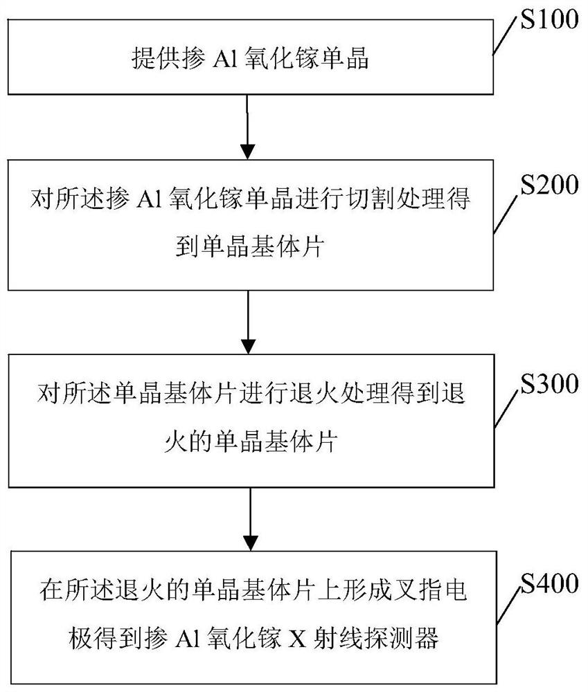
[0044] like figure 1 Shown, a kind of preparation method of Al-doped gallium oxide X-ray detector of the present invention comprises the following steps:
[0045] Step S100, providing an Al-doped gallium oxide single crystal.
[0046] Specifically, X-rays are electromagnetic radiation with energy between ultraviolet light and γ-rays. X-ray detection technology is based on the interaction between X-rays and matter to produce photoconductive or ionized excitation equivalents, generating secondary electrons and passing through the back-end electrons. Chemical processing produces electrical signals. Al-doped gallium oxide X-ray detector as a semiconductor detector uses semiconductor materials to absorb high-energy X-rays and generate electron-hole pairs, and the carriers induced by X-rays are collected by external circuits to form electrical signals. Al-doped gallium oxide single crystal refers to the single crystal formed by Al-doped gallium oxide material. Compared with galliu...
specific Embodiment 1
[0081] 1. Use the guided mode method to grow 100-face Al-doped gallium oxide, cut it to obtain a 6mm×6mm×0.5mm crystal plate, and the Al-doped concentration is 20mol%.
[0082] 2. Perform annealing treatment on the Al-doped gallium oxide substrate sheet, under the air atmosphere, the annealing temperature is 1450°C, and the annealing time is 20h.
[0083] 3. Grinding and polishing the Al-doped gallium oxide substrate after the annealing is completed.
[0084] 4. After polishing, ultrasonic treatment in acetone and ethanol in turn.
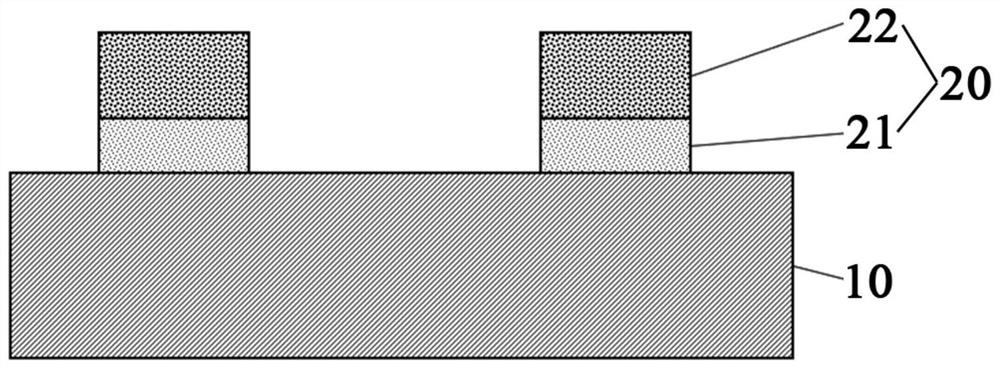
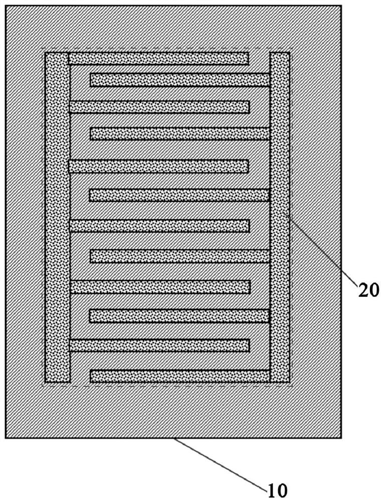
[0085] 5. Plating Ti / Au electrodes (Ti layer thickness is 10nm; Au layer electrode thickness is 50nm) interdigitated electrodes on the Al-doped gallium oxide single wafer, with a width and interval of 100 μm, using magnetron sputtering coating.
[0086] 6. Under the voltage of 1v, excite the X-ray every 30s, and test the response time of the device. Specific results such as Figure 4 shown. It can be seen that the stress response time of the Al...
specific Embodiment 2
[0088]In order to verify the impact of the annealing treatment on the Al-doped gallium oxide X-ray detector, prepare the Al-doped gallium oxide X-ray detector without annealing treatment, except that the annealing treatment is not performed, the steps of the second embodiment and the specific embodiment Step 1 is the same.
[0089] like Figure 5 As shown, the sensitivity of the Al-doped gallium oxide X-ray detector is obviously less than the sensitivity of the Al-doped gallium oxide X-ray detector in the present invention, and the response time of the Al-doped gallium oxide X-ray detector is 60s, which is obviously greater than that of the present invention Response time of moderately Al-doped gallium oxide X-ray detectors. Moreover, the current of the Al-doped gallium oxide X-ray detector in the present invention is smaller than that of the non-Al-doped gallium oxide X-ray detector.
[0090] It should be noted that when testing the device performance, the device can also b...
PUM
| Property | Measurement | Unit |
|---|---|---|
| thickness | aaaaa | aaaaa |
| thickness | aaaaa | aaaaa |
| length | aaaaa | aaaaa |
Abstract
Description
Claims
Application Information


