Correction method of square resistance in ohmic contact area

An ohmic contact area and ohmic contact technology, applied in the measurement of resistance/reactance/impedance, circuits, electrical components, etc., can solve problems such as large amount of calculation, inability to do approximate processing, and influence of the accuracy of the square resistance value in the ohmic area. The process technology is simple and stable, the test method is fast and convenient, and it is conducive to the effect of process optimization

Active Publication Date: 2017-10-13
XIDIAN UNIV
View PDF5 Cites 7 Cited by
  • Summary
  • Abstract
  • Description
  • Claims
  • Application Information

AI Technical Summary

Problems solved by technology

There are several problems in this method: firstly, since complex processes such as metal deposition and high-temperature annealing are implemented on the ohmic contact area, the sheet resistance of the active area and the ohmic contact area are not equal, or even very different. It cannot be approximated; secondly, the rectangular transmission line model has fringe current effects, so the use of this model has a certain impact on the accuracy of the square resistance value in the ohmic region
There are several problems with this method: first, the traditional CTLM method ignores the sheet resistance of the metal layer during measurement, which will have a certain impact on the experimental results; The difference between the resistance values ​​of these parts is very small, and the error is relatively large after the difference is made; moreover, the formula for directly calculating the square resistance in the ohmic area is more complicated, the amount of calculation is large, and it involves the calculation of trigonometric functions at non-special angles, so the test and The total time for calculation and analysis is long
[0007] With the further development of semiconductor devices, the original ohmic contact area sheet resistance measurement method is becoming more and more difficult to meet the requirements of high-performance semiconductor device development

Method used


Image

  • Correction method of square resistance in ohmic contact area
  • Correction method of square resistance in ohmic contact area
  • Correction method of square resistance in ohmic contact area

Examples


Embodiment Construction

[0032] The specific implementation of the present invention will be further described in detail below in conjunction with the accompanying drawings and examples. The following examples are used to illustrate the present invention, but are not intended to limit the scope of the present invention.

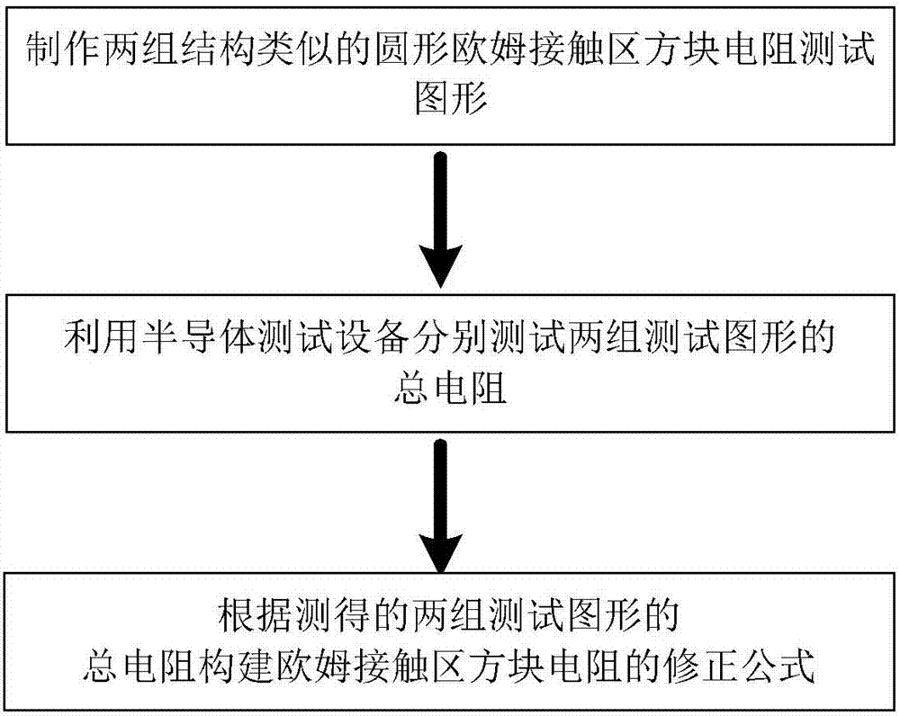
[0033] refer to figure 1 , the implementation steps of the present invention are as follows:

[0034]Step 1, make the test pattern of the square resistance of the ohmic contact area.

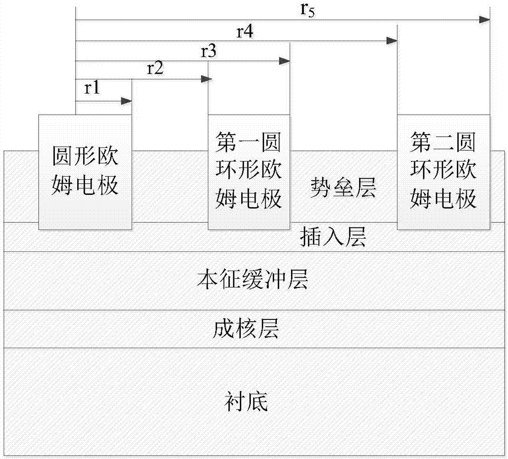
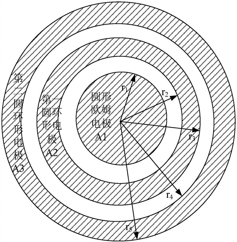
[0035] refer to figure 2 , the specific implementation of this step is as follows:

[0036] 1a) Using the heterojunction epitaxial growth method to grow the substrate layer, nucleation layer, intrinsic buffer layer, insertion layer, and barrier layer sequentially from bottom to top on the substrate; the commonly used substrates are sapphire, silicon, and silicon carbide , diamond and other materials, the nucleation layer and the insertion layer are commonly used aluminum nitride materials, the com...


PUM


Abstract

The invention discloses a testing and correction method of a square resistance in an ohmic contact area for mainly solving the problems of inaccurate calculation and complex calculation process of the square resistance Rshc in the ohmic contact area in the prior art. The realization scheme comprises the steps of manufacturing two groups of similar round ohmic contact testing patterns, wherein each group comprises a round ohmic electrode and two concentric ring-shaped ohmic electrodes; then testing the total resistance of the two groups of the round testing patterns, respectively; and correcting the value of the square resistance Rsh in an active area by utilizing a correction formula so as to further calculate the value of the square resistance Rshc in the ohmic contact area accurately. The correction method of the square resistance in the ohmic contact area has the advantages of simple and easily-manufactured testing patterns, simple calculation and accurate result, and can be used for technology detection and performance evaluation of semiconductor devices.

Description

technical field [0001] The invention belongs to the technical field of testing, and in particular relates to a method for correcting the square resistance of an ohmic contact area, which can be used in the preparation, performance evaluation and reliability analysis of heterojunction transistors. Background technique [0002] Wide-bandgap semiconductor materials represented by III-V materials have many advantages, and their development has been quite rapid in recent years. Semiconductor devices made of this type of material have excellent advantages such as high electron mobility, wide band gap, high thermal conductivity, high pressure resistance, high temperature resistance, and radiation resistance, and can be widely used in high temperature, high power, optoelectronics, high frequency microwave and mm Wave and other fields have a broad market. Therefore, in recent years, this type of related devices has become a research hotspot both at home and abroad. [0003] In the ...

Claims


Application Information

Patent Timeline
Patent Type & Authority Applications(China)
IPC IPC(8): H01L21/66
CPCH01L22/14H01L29/401H01L22/34H01L21/28575H01L29/2003G01R27/205H01L21/283H01L21/26546H01L21/3245H01L29/778H01L29/66462H01L29/41758
Inventor 郑雪峰董帅帅王士辉吉鹏白丹丹文浩宇王奥琛王冲郝跃
Owner XIDIAN UNIV
Why Eureka
Try Eureka