Manufacturing method of compound semiconductor MIM (Metal Injection Molding) capacitor structure

A technology of capacitor structure and manufacturing method, which is applied in the direction of semiconductor devices, semiconductor/solid-state device parts, capacitors, etc., can solve the problems of high cost, large circuit area, and increasing the area of ​​capacitor integrated circuits, so as to increase the capacitance value, The effect of improving overall performance

Active Publication Date: 2017-11-10
XIAMEN SANAN INTEGRATED CIRCUIT
View PDF4 Cites 1 Cited by
  • Summary
  • Abstract
  • Description
  • Claims
  • Application Information

AI Technical Summary

Problems solved by technology

[0003] In order to increase the capacity of the capacitor, the prior art often adopts the method of increasing the area of ​​the electrode plate of the capacitor, which obviously increases the area of ​​the integrated circuit occupied by the capacitor an

Method used


Image

  • Manufacturing method of compound semiconductor MIM (Metal Injection Molding) capacitor structure
  • Manufacturing method of compound semiconductor MIM (Metal Injection Molding) capacitor structure

Examples


Embodiment Construction

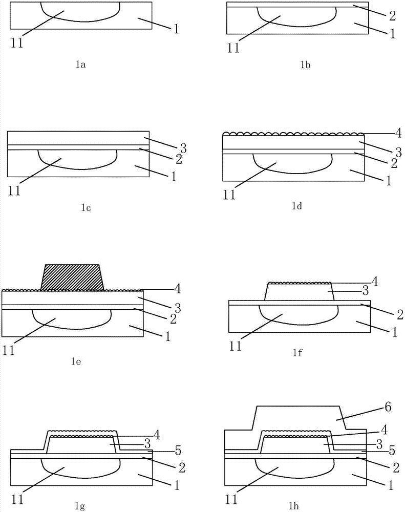
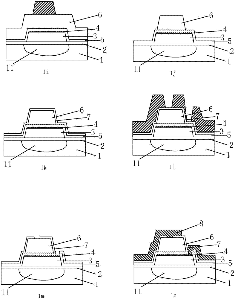
[0026] The present invention will be described in further detail below in conjunction with the accompanying drawings and embodiments. The drawings of the present invention are only schematic diagrams for easier understanding of the present invention, and their specific proportions can be adjusted according to design requirements. Those skilled in the art should understand that the upper and lower relationships of relative components in the figures described herein refer to the relative positions of the components, so all of them can be turned over to present the same components, which should all fall within the scope of the present specification. In addition, the number of elements and structures, the thickness of layers and the comparison of thicknesses between layers shown in the figure are only examples and are not limited thereto, and can be adjusted according to actual design requirements.

[0027] The following examples specifically illustrate a method for making a compo...


PUM

PropertyMeasurementUnit
Thicknessaaaaaaaaaa
Thicknessaaaaaaaaaa
Thicknessaaaaaaaaaa

Abstract

The invention discloses a manufacturing method of a compound semiconductor MIM (Metal Injection Molding) capacitor structure. The method comprises the following steps: performing insulating treatment on a compound semiconductor wafer, and depositing a polycrystalline silicon layer; depositing a rough polycrystalline silicon layer through the polycrystalline silicon layer under the oxidation action of diluted ammonia water; then, forming a lower polar plate of an MIM capacitor through a photolithographic process; forming a dielectric layer and an upper polar plate in sequence by depositing; and then making a metal connection line. Through deposition of rough polycrystalline silicon, an uneven structure is formed on the surface of the lower polar plate, and the effective area of the polar plate can be 1.5 to 2.5 times of a plane area, so that the capacitance value of the capacitor is increased effectively on the premise of not changing the overall floor area of the MIM capacitor, and the overall performance of the MIM capacitor is improved. Through adoption of the method, certain physical characteristics in a compound semiconductor are overcome, and an effective implementation mode is provided for the integrated circuit arrangement and performance improvement of the compound semiconductor.

Description

technical field [0001] The invention relates to semiconductor technology, in particular to a manufacturing method of a semiconductor MIM capacitance structure and the capacitance structure thereof. Background technique [0002] MIM capacitors are widely used as charge storage, coupling and filter devices, and their production is an important process link in the production process of semiconductor integrated circuits. A conventional MIM capacitor includes upper and lower electrode plates and a dielectric layer sandwiched between them, and the capacitance of the capacitor is proportional to the area of ​​the electrode plates. With the development of microelectronics technology, in order to improve the overall performance of semiconductor devices to achieve faster computing speed, larger data storage capacity and more functions, the capacity requirements of capacitors are increasing day by day. [0003] In order to increase the capacity of the capacitor, the prior art often ad...

Claims


Application Information

Patent Timeline
IPC IPC(8): H01L23/64
CPCH01L23/642H01L28/84
Inventor 王勇
Owner XIAMEN SANAN INTEGRATED CIRCUIT
Why Eureka
Try Eureka