

Sapphire substrate nanopore preparation method
A sapphire substrate and nanohole technology, applied in electrical components, circuits, semiconductor devices, etc., can solve the problems of poor repeatability, high processing cost, low efficiency, etc., and achieve improved light extraction efficiency and controllable duty cycle. , cycle controllable effect
- Summary
- Abstract
- Description
- Claims
- Application Information
AI Technical Summary
Problems solved by technology
Method used
Image


Examples
Embodiment Construction
[0026] Hereinafter, embodiments of the present invention will be described in detail with reference to the accompanying drawings. This invention may, however, be embodied in many different forms and should not be construed as limited to the specific embodiments set forth herein. Rather, the embodiments are provided to explain the principles of the invention and its practical application, thereby enabling others skilled in the art to understand the invention for various embodiments and with various modifications as are suited to particular intended uses.
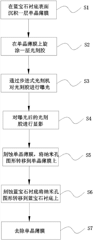
[0027] refer to figure 1 , and combined with Figure 2 to Figure 7 As shown, the present embodiment provides a method for preparing nanopores on a sapphire substrate, the method comprising the following steps:
[0028] Step S1: Deposit a single crystal film 2 on the surface of the sapphire substrate 1, the single crystal film 2 is a silicon dioxide single crystal film with a thickness of 200nm to 300nm, such as figure 2 S...
PUM
| Property | Measurement | Unit |
|---|---|---|
| thickness | aaaaa | aaaaa |
Abstract
Description
Claims
Application Information