Reaction cavity and semiconductor processing device

A reaction chamber and reaction gas technology, which is applied in the manufacture of semiconductor/solid-state devices, discharge tubes, electrical components, etc., can solve the problems of uneven distribution of electromagnetic field, uneven voltage distribution, and large voltage difference, so as to achieve the goal of weakening the electric field. The effect of uniformity, the effect of improving the uniformity of density distribution, and the effect of improving the uniformity of electric field

Active Publication Date: 2017-11-21
BEIJING NAURA MICROELECTRONICS EQUIP CO LTD
View PDF3 Cites 7 Cited by
  • Summary
  • Abstract
  • Description
  • Claims
  • Application Information

AI Technical Summary

Problems solved by technology

[0005] First, due to the influence of the coil structure, the high-frequency electric field generated by the coil tends to have an M-shaped distribution. This distribution causes the density of the plasma generated in the reaction chamber to also show an M-shaped distribution, resulting in plasma on the surface of the wafer. Uneven density distribution, which affects process uniformity
[0006] Second, because the output terminal of the coil is grounded, the voltage difference between the output terminal and the input terminal of the coil is relatively large, resulting in uneven distribution of voltage along the surface of the coil, resulting in uneven distribution of the electromagnetic field generated by the coil
Although the method of connecting a capacitor in series between the output end of the coil and the ground end can be used to make the voltage between the output end of the coil and the input end consistent, but in fact, this method cannot really make the output end of the coil and the ground end. The voltage between the input terminals is consistent, because: during the process, there is capacitive coupling between the coil and the plasma, and the effect of this capacitive coupling causes the capacitance connected in series between the output terminal of the coil and the ground terminal The value changes with the change of discharge conditions, resulting in a large deviation between the actual capacitance value and the required capacitance value between the output end of the coil and the ground end in series, and then the output end of the coil and the input end. The voltage difference between them is relatively large, so there is still the problem of uneven distribution of the electromagnetic field generated by the coil

Method used


Image

  • Reaction cavity and semiconductor processing device
  • Reaction cavity and semiconductor processing device
  • Reaction cavity and semiconductor processing device

Examples


Embodiment Construction

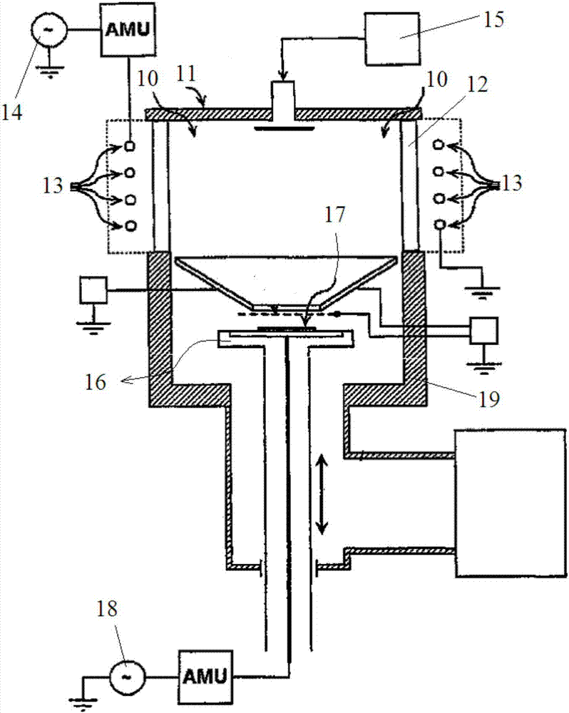
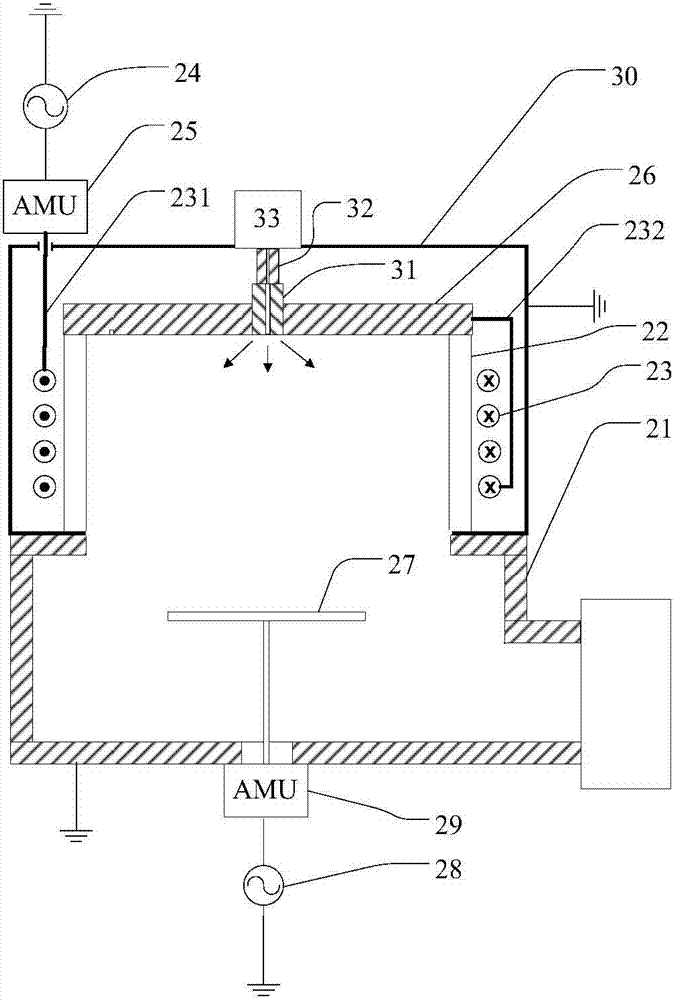
[0032] In order for those skilled in the art to better understand the technical solution of the present invention, the reaction chamber and semiconductor processing equipment provided by the present invention will be described in detail below in conjunction with the accompanying drawings.

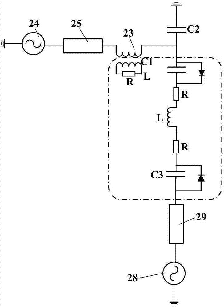
[0033] Figure 2A A cross-sectional view of the reaction chamber provided by the first embodiment of the present invention. see Figure 2A , the reaction chamber includes an upper electrode device and a lower electrode device. Wherein, the upper electrode device includes a dielectric cylinder 22, a coil 23, an upper power supply 24, a first matching device 25, and an upper electrode assembly. The lower electrode device includes a base 27 , a lower power supply 28 , and a second matcher 29 .

[0034] Wherein, the chamber wall 21 of the reaction chamber is grounded, and the chamber wall 21 surrounds and forms a cavity structure with an opening at the top; the medium cylinder 22 is arranged...


PUM


Abstract

The present invention provides a reaction cavity and a semiconductor processing device. The reaction cavity comprises a top electrode device and a bottom electrode device, and the bottom electrode device is arranged in the reaction cavity and configured to bear a wafer. The top electrode device comprises a medium cylinder, a coil, a top power source and a top electrode module, and the medium cylinder is arranged at the top of the reaction cavity; the coil is around and arranged at the periphery of the medium cylinder; the top electrode device comprises a top electrode plate, and the top electrode plate is arranged at the top of the medium cylinder; and the top power source is configured to load excitation power to the top electrode plate and the coil at the same time. The reaction cavity can reduce the voltage difference between the output end and the input end of the coil and can weaken the influence generated by a nonuniform electric field so as to improve the plasma density distribution uniformity.

Description

technical field [0001] The invention relates to the field of semiconductor manufacturing, in particular to a reaction chamber and semiconductor processing equipment. Background technique [0002] In the semiconductor field, for dry etching process and thin film deposition process, commonly used plasma sources include inductively coupled plasma (Inductive Coupled Plasma, hereinafter referred to as ICP) source and capacitive coupled plasma (hereinafter referred to as CCP) )source. Among them, the ICP source uses the electromagnetic field generated by the current passing through the coil to excite the reactive gas to generate plasma. The ICP source has the characteristics of high plasma density and small damage to the workpiece. The CCP source excites the reactive gas to generate plasma by the voltage applied between the electrode plates. The CCP source has the characteristics of large area uniformity and high ion energy. [0003] figure 1 Cross-sectional view of the reactio...

Claims


Application Information

Patent Timeline
Patent Type & Authority Applications(China)
IPC IPC(8): H01J37/32H01L21/265H01L21/67
CPCH01J37/32H01J37/32807H01L21/265H01L21/67H01L21/67011
Inventor 李兴存韦刚成晓阳苏恒毅
Owner BEIJING NAURA MICROELECTRONICS EQUIP CO LTD
Why Eureka
Try Eureka