Manufacturing method of controllable-temperature microfluidic chip

A technology of microfluidic chips and manufacturing methods, applied in chemical instruments and methods, laboratory containers, laboratory utensils, etc., can solve problems such as limited heat transfer capacity, complex device structure, and increased maintenance difficulty. The effect of high control precision and fast heating and cooling speed

Active Publication Date: 2017-11-24
上海萃励电子科技有限公司
View PDF8 Cites 5 Cited by
  • Summary
  • Abstract
  • Description
  • Claims
  • Application Information

AI Technical Summary

Problems solved by technology

At present, microfluidic chips that require low-temperature operation usually use commercial semiconductor cooling chips to be placed under the chip for cooling operations. Due to the limitations of the semiconductor cooling chip packaging ceramics and the heat transfer capacity of the microfluidic chip material itself, the temperature control effect is especially high. There is still a big bottleneck in the ability of rapid heating and cooling during the flux detection process
The patent (CN105914189A) discloses a microfluidic chip cooling device, which uses a combination of a semiconductor cooling chip and a cavity filled with a liquid metal heat-conducting medium to improve cooling efficiency, but the structure of the device is complex, and it also violates the principle of all-solid-state cooling of thermoelectric semiconductor materials. The original intention of the design increases the difficulty of maintenance again
[0004] In addition, due to the multi-unit operation of chemical or biological processes on tiny chips, different units often have different temperature requirements. The simple superposition of existing semiconductor chips and microfluidic chips cannot achieve precise temperature control for each area.

Method used


Image

  • Manufacturing method of controllable-temperature microfluidic chip
  • Manufacturing method of controllable-temperature microfluidic chip
  • Manufacturing method of controllable-temperature microfluidic chip

Examples


Embodiment 1

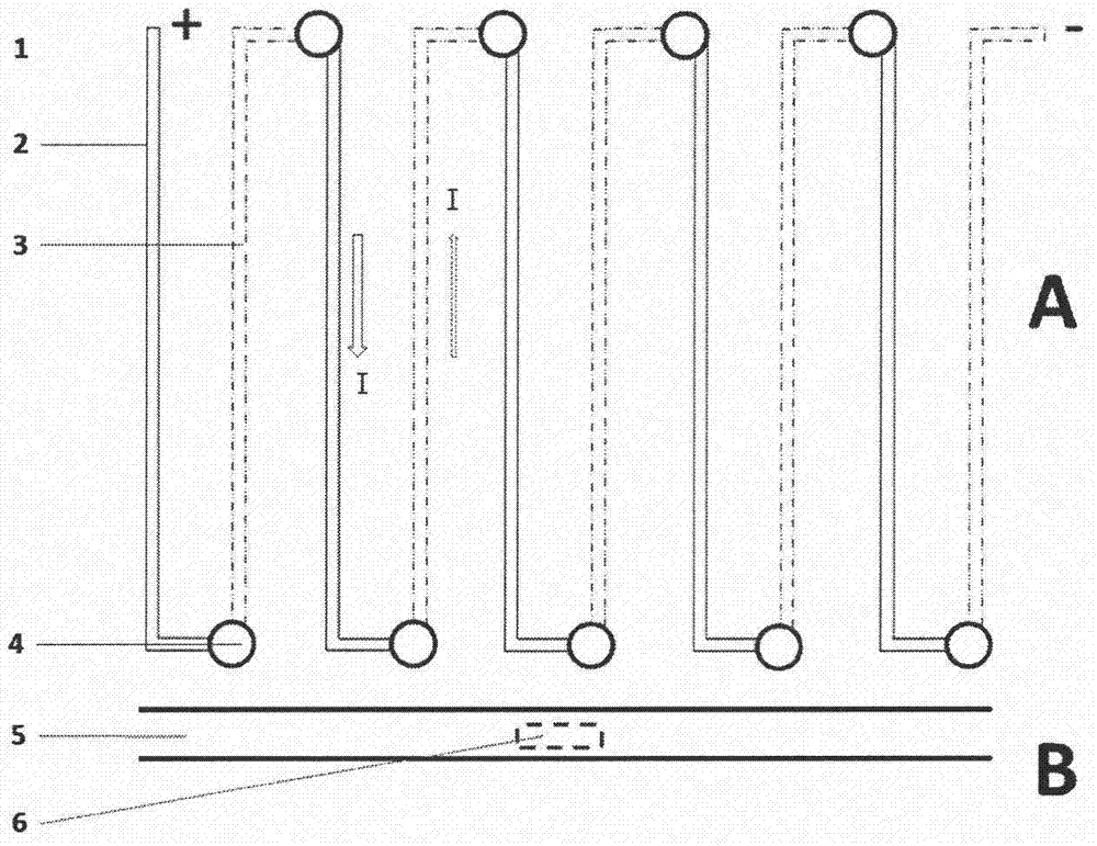
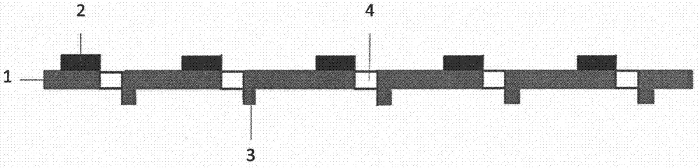
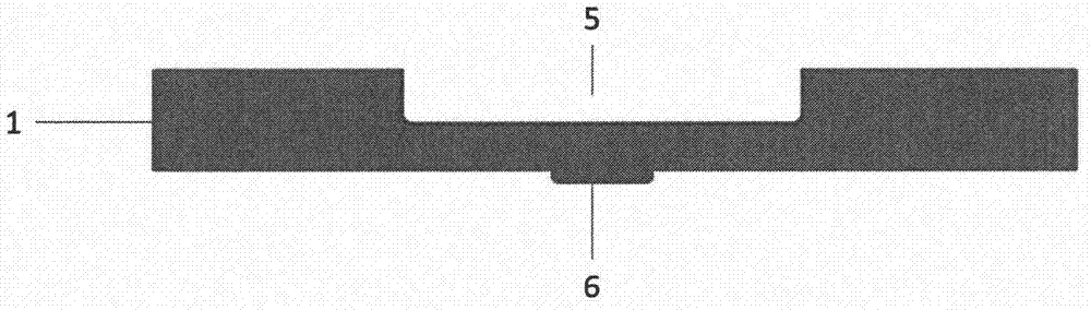
[0025] designed as figure 1 The temperature-controllable microfluidic chip shown has a planned reaction groove area and a temperature-controlled circuit area. The substrate adopts an alumina ceramic substrate, and a reaction groove is processed by laser ablation on one side of the reaction groove area, and a thermocouple temperature measuring probe is printed on the back of the reaction groove. N-type Bi sputtered by mask magnetron sputtering on the front side of the temperature control line area 0.5 Sb 1.5 Te 3 Circuit layer of thermoelectric material, P-type Bi2Te sputtered by mask magnetron sputtering on the back 2.7 Se 0.3 For the circuit layer of thermoelectric materials, through holes are drilled in the line section, and copper is electroplated in the through holes to form an alternating series circuit structure of N-P-N-P..., such as figure 1 When the circuit is connected as shown, the cooling of the reaction tank is realized. The schematic diagram of the cross-se...

Embodiment 2

[0027] designed as figure 1 The temperature-controllable microfluidic chip shown has a planned reaction groove area and a temperature-controlled line area. The substrate adopts a silicon substrate, a groove for reaction is processed by mask photolithography on one side of the reaction groove area, and a thermocouple temperature measuring probe is printed on the back of the reaction groove. On the front side of the temperature control circuit area, the circuit layer of N-type PbTe thermoelectric material is vacuum-evaporated, and the circuit layer of P-type PbSe thermoelectric material is vacuum-evaporated on the back. Through holes are drilled in the line section, and silver is electroplated in the through holes to form Alternating series line structure of N-P-N-P…, such as figure 1 When the circuit is connected as shown, the cooling of the reaction tank is realized. The schematic diagram of the cross-sectional structure of the through hole in the temperature control circuit...

Embodiment 3

[0029] designed as figure 1 The temperature-controllable microfluidic chip shown has a planned reaction groove area and a temperature-controlled line area. The substrate adopts a hard polyimide substrate, and a groove for reaction is processed by hot molding on one side of the reaction groove area, and an NTC temperature measuring probe is printed on the back of the reaction groove. In the temperature control line area, the circuit layer of N-type Bi paste thermoelectric material is screen-printed on the front side, and the circuit layer of P-type BiSb paste thermoelectric material is screen-printed on the back side. After drying, through holes are drilled in the line section. Gold is electroplated in the through hole to form an alternating series circuit structure of N-P-N-P..., such as figure 1 When the circuit is connected as shown, the cooling of the reaction tank is realized. The schematic diagram of the cross-sectional structure of the through hole in the temperature c...


PUM


Abstract

The invention discloses a manufacturing method of a controllable-temperature microfluidic chip. The method is characterized by comprising the following steps: printing a thermoelectric semiconductor temperature control circuit on the upper plane of the microfluidic chip, wherein the chip comprises at least one reaction groove area and at least one temperature control circuit area; processing a reaction groove one surface of the reaction groove area, and printing a temperature sensing probe on the rear surface of the other surface of the reaction groove; correspondingly printing circuit layers which are correspondingly manufactured through an N type thermoelectric material and a P type thermoelectric material on two surfaces of the chip at the temperature control circuit area; forming an N-P-N-P...alternative series-connection circuit structure through copper plating through holes; and connecting a power supply to refrigerate and heat the reaction groove area. The method has the advantages that the temperature of the groove reactor area of the microfluidic chip can be accurately controlled; the temperature control accuracy is high; the temperature is rapidly increased; and the method is applicable to high-flux biological detection and multi-temperature-section complex micro-reaction process study.

Description

technical field [0001] The invention relates to a method for manufacturing a temperature-controllable microfluidic chip, which belongs to the field of electronic devices and micro-nano processing. Background technique [0002] A microfluidic chip refers to a chemical or biological laboratory built on a centimeter-square chip. The basic operations can be integrated on a very small chip, and the microchannels form a network to control the fluid passing through the system, so as to realize chemical synthesis, biological detection and other functions. The main feature of a microfluidic chip is that the effective structures (channels, reaction chambers, etc.) containing fluids are microscale or nanoscale in at least one dimension. In the process of chemical reaction or biological detection, it is usually necessary to precisely control the temperature of the reaction process. For example, in the process of gene sequencing PCR detection, it is necessary to cycle the heat preservat...

Claims


Application Information

Patent Timeline
Patent Type & Authority Applications(China)
IPC IPC(8): B01L3/00
CPCB01L3/502707B01L2300/1805
Inventor 汪元元
Owner 上海萃励电子科技有限公司
Why Eureka
Try Eureka