Double-face capacitor and manufacturing method thereof

A manufacturing method and capacitor technology, applied in the direction of electric solid-state devices, circuits, electrical components, etc., can solve problems that affect the connection between capacitors and other chip metals and the stability of packaging applications, reduce the overall performance of capacitor arrays, and limit the increase in capacitance values. Achieve high mechanical strength, increase capacitance value, and improve the effect of capacitance value

Inactive Publication Date: 2017-11-24
CHANGXIN MEMORY TECH INC
View PDF5 Cites 16 Cited by
  • Summary
  • Abstract
  • Description
  • Claims
  • Application Information

AI Technical Summary

Problems solved by technology

[0003] Most of the capacitors in the existing DRAM have a single-sided capacitor structure, which severely limits the improvement of the capacitance value per unit area.
[0004] In addition, the existing capacitor array usually adopts the masking layer 20 of the rectangular window 22 to deal with the margin, such as figure 2 As shown, the masking layer of such a

Method used


Image

  • Double-face capacitor and manufacturing method thereof
  • Double-face capacitor and manufacturing method thereof
  • Double-face capacitor and manufacturing method thereof

Examples


Embodiment Construction

[0068] The following describes the implementation of the present invention through specific specific examples. Those skilled in the art can easily understand other advantages and effects of the present invention from the content disclosed in this specification. The present invention can also be implemented or applied through other different specific embodiments, and various details in this specification can also be modified or changed based on different viewpoints and applications without departing from the spirit of the present invention.

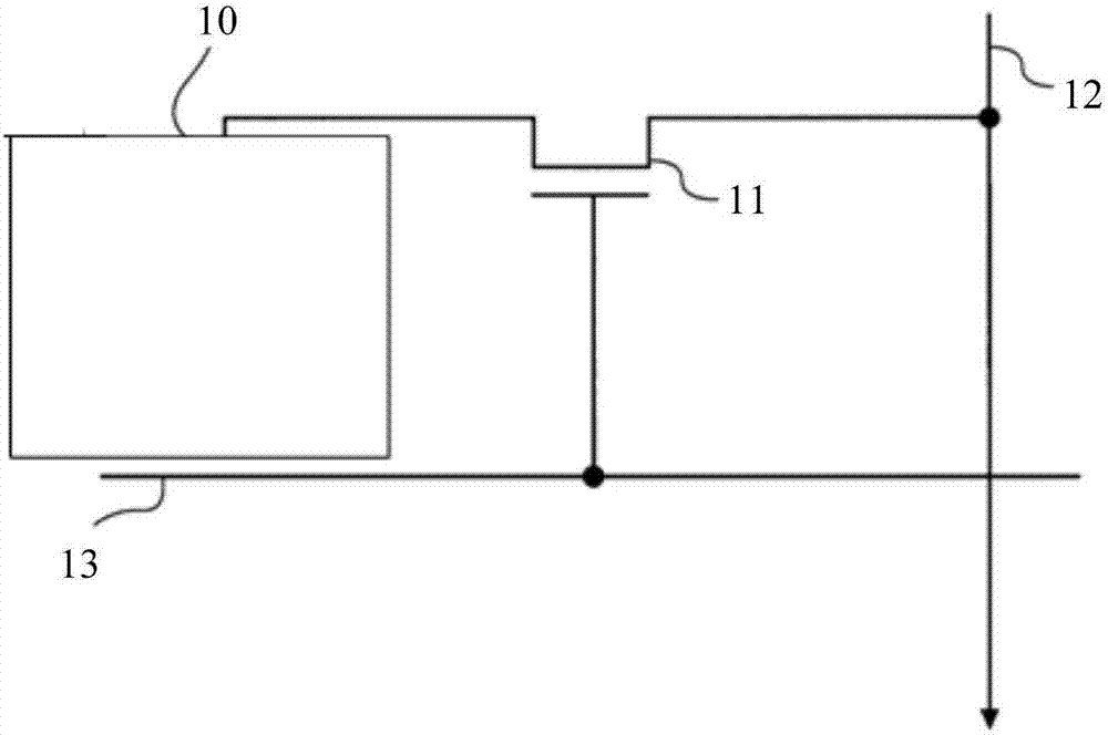
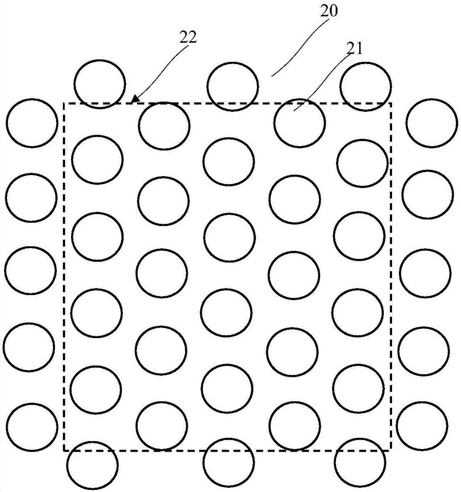
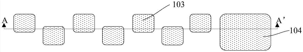
[0069] See Figure 3a~Figure 23 . It should be noted that the diagrams provided in this embodiment only illustrate the basic idea of ​​the present invention in a schematic way, so the diagrams only show the components related to the present invention instead of the number, shape, and shape of the components in actual implementation. For size drawing, the type, quantity, and proportion of each component can be changed at will during actual imp...


PUM

PropertyMeasurementUnit
Heightaaaaaaaaaa

Abstract

The invention provides a double-face capacitor and a manufacturing method thereof. The double-face capacitor includes: a semiconductor substrate, wherein multiple pads in memory array structures are formed on the semiconductor substrate; and a double-face capacitor array, which is formed on the first pad, wherein each double-face capacitor includes a first double-U conductive layer, a second double-U conductive layer, a capacitor dielectric, and a third conductive layer. Through a multi-pattern method and a support frame structure strengthened by a boundary process, the hexagonal-array-arranged double-face capacitor with a double-U bottom electrode is manufactured. The capacitor has a great height and a great width ratio, and is effectively improved in capacitance value per unit area.

Description

Technical field [0001] The invention belongs to the field of semiconductor devices and manufacturing, and particularly relates to a double-sided capacitor and a manufacturing method thereof. Background technique [0002] Dynamic random access memory (Dynamic Random Access Memory, referred to as: DRAM) is a semiconductor storage device commonly used in computers, which is composed of many repeated memory cells. Each memory cell usually includes a capacitor 10 and a transistor 11; the gate of the transistor 11 is connected to the word line 13, the drain is connected to the bit line 12, and the source is connected to the capacitor 10; the voltage signal on the word line 13 can control the transistor 11 Turn on or off, and then read the data information stored in the capacitor 10 through the bit line 12, or write the data information to the capacitor 10 through the bit line 12 for storage, such as figure 1 Shown. [0003] Most of the capacitors in the existing dynamic random access me...

Claims


Application Information

Patent Timeline
IPC IPC(8): H01L23/64H01L27/108
CPCH01L23/642H10B12/30
Inventor 不公告发明人
Owner CHANGXIN MEMORY TECH INC
Why Eureka
Try Eureka