Heterojunction resistive switching memory and manufacturing method thereof

A technology of resistive memory and heterojunction, applied in electrical components and other directions, can solve the problems of difficulty in meeting high storage density, difficult practical application, complex process, etc., and achieve the effects of easy preparation, stable memristive behavior and low cost.

Active Publication Date: 2017-12-05
XIDIAN UNIV
View PDF3 Cites 6 Cited by
  • Summary
  • Abstract
  • Description
  • Claims
  • Application Information

AI Technical Summary

Problems solved by technology

Although these resistive switching materials can have good resistive switching characteristics under a specific preparation process, the preparation process is relatively complicated, and the commonly used high-temperature trea

Method used


Image

  • Heterojunction resistive switching memory and manufacturing method thereof
  • Heterojunction resistive switching memory and manufacturing method thereof
  • Heterojunction resistive switching memory and manufacturing method thereof

Examples


Embodiment 1

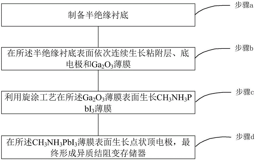
[0041] See figure 1 , figure 1 It is a schematic diagram of a manufacturing method of a heterojunction resistive memory provided by an embodiment of the present invention. The method comprises the steps of:

[0042] Step a, preparing a semi-insulating substrate;

[0043] Step b, continuously growing an adhesion layer, a bottom electrode and Ga on the surface of the semi-insulating substrate 2 o 3 film;

[0044] Step c, using a spin coating process on the Ga 2 o 3 Growth of CH on the film surface 3 NH 3 PB 3 film;

[0045] Step d, in the CH 3 NH 3 PB 3 Dot-shaped top electrodes are grown on the surface of the film to form a heterojunction resistive variable memory.

[0046] Wherein, step a may include:

[0047] Growth of SiO on Si Substrate Surface by Thermal Oxidation Process 2 to prepare the semi-insulating substrate.

[0048] Further, after step a, it may also include:

[0049] The semi-insulating substrate was washed sequentially for 5 min with acetone sol...

Embodiment 2

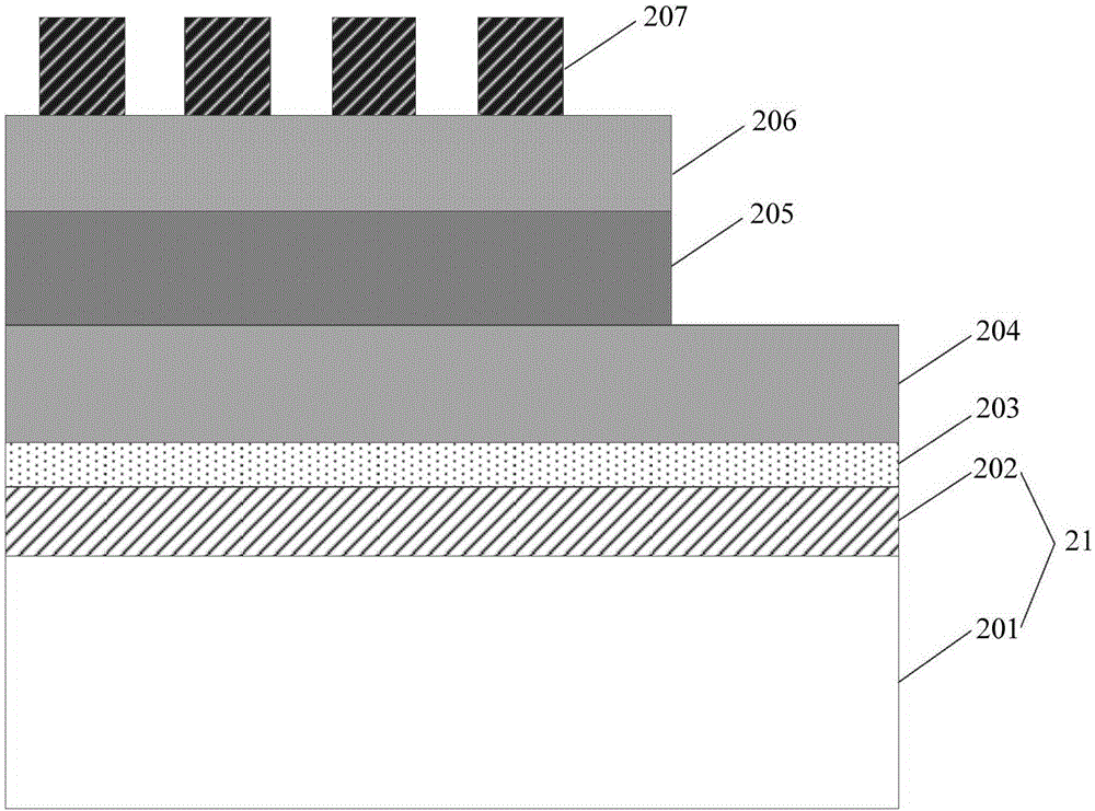
[0067] See figure 2 , figure 2 It is a device schematic diagram of a heterojunction resistive memory provided by an embodiment of the present invention. The heterojunction resistive variable memory includes: a semi-insulating substrate 21, an adhesion layer 203, a bottom electrode 204, Ga 2 o 3 Film 205, CH 3 NH 3 PB 3 Thin film 206 and dot-like top electrode 207; Wherein, semi-insulating substrate 21 is made of Si substrate 201 and SiO produced by thermal oxidation on the surface of Si substrate 2 202, and the heterojunction resistive variable memory is prepared by the method described in the above embodiment.

[0068] Preferably, Ga 2 o 3 Thin film is N-type, CH 3 NH 3 PB 3 Thin film is P-type, N-type Ga 2 o 3 Thin films and P-type CH 3 NH 3 PB 3 The thin film forms a laminated PN heterojunction resistive layer.

[0069] The transistor of the present invention adopts CH 3 NH 3 PB 3 Provide a large number of electrons to the channel to form an n-type MO...

Embodiment 3

[0071] See Figure 3a ~ Figure 3f , Figure 3a ~ Figure 3f A process flow diagram of a heterojunction resistive memory provided by an embodiment of the present invention. This embodiment describes the technical solution of the present invention in detail on the basis of the above embodiments. Specifically, the method may include:

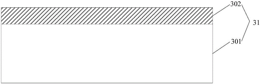
[0072] Step 1: Select a semi-insulating substrate.

[0073] Select Si substrate 301, and use thermal oxidation process to grow SiO on the surface of Si substrate 2 302 forms a semi-insulating substrate 31, SiO 2 The thickness of 302 is 80nm-120nm; the semi-insulating substrate 31 is cleaned to remove surface pollutants and natural oxide layer; the cleaning process is as follows: the semi-insulating substrate is placed in an acetone solution for ultrasonic cleaning for 5 minutes to remove surface pollutants, and then Ultrasonic cleaning with ethanol and deionized water for 5 min each, such as Figure 3a said;

[0074] Preferably, SiO 2 The ...


PUM

PropertyMeasurementUnit
Thicknessaaaaaaaaaa
Thicknessaaaaaaaaaa
Thicknessaaaaaaaaaa

Abstract

The invention relates to a heterojunction resistive switching memory and a manufacturing method thereof. The method comprises steps: a semi-insulating substrate is manufactured; an adhesion layer, a bottom electrode and a Ga2O3 film grow on the surface of the semi-insulating substrate sequentially; a spin coating process is used to grow a CH3NH3PbI3 film on the surface of the Ga2O3 film; and a point-shaped top electrode grows on the surface of the CH3NH3PbI3 film, and the heterojunction resistive switching memory is finally formed. as the resistive switching layer adopts the heterojunction, modulation is easy, the memory and relaxation process of a resistor is regulated by factors such as the width of a depletion layer and the strength of an internal electric field, and the memristor performance regulation flexibility is enhanced; and selectivity for materials is weak, the performance of the memristor behavior is stable, semi-quantification research on the memristor is facilitated, and a basis is laid for device design and further development.

Description

technical field [0001] The invention relates to the technical field of integrated circuits, in particular to a heterojunction resistive variable memory and a preparation method thereof. Background technique [0002] Semiconductor integrated circuits are the foundation of the electronics industry, and people's huge demand for the electronics industry has prompted the rapid development of this field. In the past few decades, the rapid development of the electronics industry has had a huge impact on social development and national economy. With the development of integrated circuit technology, the integration and performance of microelectronic chips are constantly improving following Moore's law, and integrated circuit technology is constantly approaching its physical limit. With the continuous progress of the information age, the demand for information storage will increase. It has become larger and larger, and the traditional Flash memory has reached its limit. As the thickn...

Claims


Application Information

Patent Timeline
IPC IPC(8): H01L45/00
CPCH10N70/881H10N70/8833H10N70/011
Inventor 贾仁需董林鹏栾苏珍庞体强张玉明汪钰成刘银涛
Owner XIDIAN UNIV
Why Eureka
Try Eureka