Superjunction reverse conducting-insulated gate bipolar transistor (IGBT) with collector groove

A collector and reverse conduction technology, applied in circuits, electrical components, semiconductor devices, etc., can solve problems such as uneven current distribution and poor diode characteristics, achieve fast turn-off speed, eliminate snapback effect, and eliminate voltage foldback Effect

Inactive Publication Date: 2017-12-12
UNIV OF ELECTRONICS SCI & TECH OF CHINA
View PDF5 Cites 14 Cited by
  • Summary
  • Abstract
  • Description
  • Claims
  • Application Information

AI Technical Summary

Problems solved by technology

However, this will make the length of the P collector much longer than the length of the N collector, resulting in uneven current distribution and poor diode characteristics when the RC-IGBT conducts in reverse.

Method used


Image

  • Superjunction reverse conducting-insulated gate bipolar transistor (IGBT) with collector groove
  • Superjunction reverse conducting-insulated gate bipolar transistor (IGBT) with collector groove
  • Superjunction reverse conducting-insulated gate bipolar transistor (IGBT) with collector groove

Examples


Embodiment 1

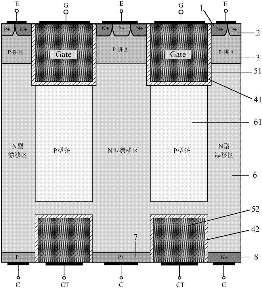
[0025] Such as figure 2 As shown, the superjunction inverse conduction IGBT with collector grooves in this example includes a MOS cell structure, an N-type drift region 6 and a collector structure from top to bottom; the MOS cell structure includes a groove gate and a P-type Well region 3; the slot gate includes a first insulating layer 41 and a first conductive material 51 located in the first insulating layer 41, and the leading end of the first conductive material 51 is a gate electrode G; the slot gate passes through the The P-type well region 3 goes deep into the N-type drift region 6; the P-type well region 3 is located on both sides of the groove gate, and the upper surface of the P-type well region 3 has an N+ emitter region 1 and a P+ body contact region 2 , and the N+ emitter region 1 is in contact with the insulating layer 41, the P+ body contact region 2 is located on both sides of the N+ emitter region 1, and the common terminal of the N+ emitter region 1 and the...

Embodiment 2

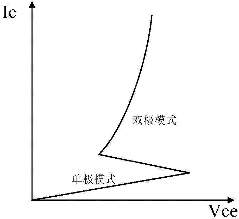
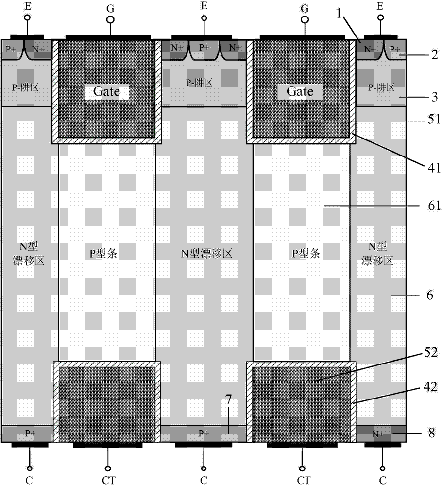
[0029] Such as image 3 As shown, the difference between this example and Example 1 is that in this example, the P-type strip 61 in the N-type drift region 6 is connected to the second insulating layer 42 of the collector groove. Compared with Example 1, in this example, the P-type strip 62 blocks the surface MOS electron current at other positions from flowing to the N+ collector region 8, and the new device is directly equivalent to a parallel connection of an IGBT and a MOS tube, thus suppressing the voltage foldback effect The effect is better.

Embodiment 3

[0031] Such as Figure 4 As shown, the difference between this example and Example 1 is that there is a voltage difference V between the second collector CT and the collector C in this example G2 . When the device is conducting forward, the voltage on the second collector CT is lower than the voltage on the collector C (that is, V G2 G2 >0), the sidewall of the second insulating layer 42 forms a high-concentration electron accumulation layer, and the electron accumulation layer and the collector groove serve as an equivalent field stop layer to ensure that the device can withstand high withstand voltage; meanwhile, the electron accumulation layer will also The potential difference between the P+ collector region 7 and the N-type drift region 6 is reduced, thereby reducing the hole injection efficiency, and it is also a channel for fast extraction of electrons, which is beneficial to improve the turn-off speed of the device. Compared with Example 1, the device in this example...


PUM


Abstract

The invention belongs to the technical field of a power semiconductor, and particularly relates to a superjunction reverse conducting-insulated gate bipolar transistor (IGBT) with a collector groove. Compared with a traditional superjunction RC-IGBT structure, the superjunction RC-IGBT has the advantages that a collector groove structure is mainly introduced to a bottom current collection region, an N drift region at the bottom of the collector groove can be consumed by P-type strips when a new device is positively conducted and does not enter a bipolar mode, so that an electron current path is occupied, the effective electron concentration is reduced, the electron current distribution resistance around the current collection region is increased, and a snapback effect of the device can be eliminated by the new device under relatively small cell size; and when the new device is switched off, the collector structure has an effect equivalent to a buffer layer, and the device can be enabled to bear high pressure. The superjunction RC-IGBT has the beneficial effects that compared with the traditional superjunction RC-IGBT structure, the snapback effect can be eliminated under smaller cell size, meanwhile, the superjunction RC-IGBT has faster switch-off speed, and the current distribution is more uniform in a reverse diode mode.

Description

technical field [0001] The invention belongs to the technical field of power semiconductors, and relates to a super junction reverse conducting IGBT (Reverse Conducting-Insulated Gate Bipolar Transistor, reverse conducting insulated gate bipolar transistor) with a collector groove. Background technique [0002] Insulated gate bipolar transistor (IGBT) combines the advantages of high input impedance and simple driving of MOSFET, as well as the advantages of high current density and low conduction voltage drop of BJT devices, and has become the core electronic component in modern power electronic circuit applications. one. Because of its unique advantages in the field of high voltage and high current, IGBT devices are widely used in transportation, smart grid, household appliances, industry, medicine, aerospace and many other fields. Because the IGBT is equivalent to a PNP transistor in the open base region when it works in reverse, it does not have a body diode like VDMOS, s...

Claims


Application Information

Patent Timeline
Patent Type & Authority Applications(China)
IPC IPC(8): H01L29/739H01L21/331H01L29/06
CPCH01L29/0603H01L29/0684H01L29/66325H01L29/7393H01L29/7397H01L29/0834H01L29/0634
Inventor 罗小蓉魏杰黄琳华邓高强孙涛赵哲言刘庆
Owner UNIV OF ELECTRONICS SCI & TECH OF CHINA
Why Eureka
Try Eureka