Method of realizing grounding circuit to improve matching characteristics of microwave multi-layer board

A technology of grounding circuit and implementation method, applied in the field of radio frequency microwave, can solve the problems of discontinuous signal return path, affecting microwave transmission performance, and unsatisfactory ground plane, etc., and achieve the effect of high promotion and application value, reduction of reflection, and simple processing and realization.

Inactive Publication Date: 2017-12-15
THE 724TH RES INST OF CHINA SHIPBUILDING IND
View PDF3 Cites 3 Cited by
  • Summary
  • Abstract
  • Description
  • Claims
  • Application Information

AI Technical Summary

Problems solved by technology

[0004] The present invention solves the problem that the ground plane in the multilayer microwave interconnection circuit substrate transmission line is not ideal, and the signal return path is discontinuous, which affects the microwave transmission performance.

Method used


Image

  • Method of realizing grounding circuit to improve matching characteristics of microwave multi-layer board
  • Method of realizing grounding circuit to improve matching characteristics of microwave multi-layer board
  • Method of realizing grounding circuit to improve matching characteristics of microwave multi-layer board

Examples


Embodiment Construction

[0012] The specific embodiment of the present invention is:

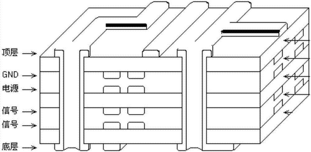
[0013] 1. For the realization of telecommunication functions and the structure determination of the installation method, carry out the layout and design of the multilayer microwave interconnection circuit substrate stack.

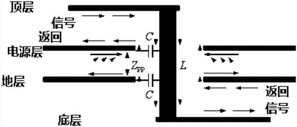
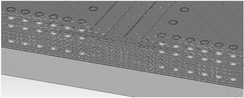
[0014] 2. Unified planning and layout design for the distribution of substrate microstrip lines, ground planes, control lines, power lines, etc. figure 1 . Build a model for 3D electromagnetic simulation of the substrate ports. Import the laminated layout file of the substrate with metallized vias into the 3D electromagnetic simulation software for modeling and simulation. Since the input impedance of the multilayer printed board signal through the metal vias to the return path of the ground plane appears extreme at the resonant frequency If the value is large, the transmission efficiency of the high-frequency signal is very low when passing through the via hole, and the coupling degree between...


PUM


Abstract

The invention relates to a method of realizing a grounding circuit to improve matching characteristics of a microwave multi-layer board. The method comprises the steps of carrying out reasonable distribution verification of metal through holes vertical to the direction of a substrate through simulation software; meanwhile through a signal return path displayed by the simulation software, interconnecting printed boards on the signal path by connecting a radio frequency ground plane with a large ground plane of the back of the multi-layer substrate in a printed board edge gilding manner; and then welding the ground plane of the back of the substrate onto a carrier of a microwave signal common ground plane to reduce the impedance between a micro-strip ground plane and the microwave signal common ground plane and thus optimize the radio frequency path performance.

Description

technical field [0001] The invention belongs to the field of radio frequency microwave technology. Background technique [0002] In the design and manufacture of active phased array radar T / R components, multi-chip components (MCM) technology is usually used to reduce the volume and improve the integration of components. It is used in multi-layer laminated microwave interconnection circuit substrates using LTCC or composite media to improve the interconnection wiring density and integration of components. Due to the difficulty and high cost of LTCC processing, the choice of printed boards is currently more inclined to use multi-layer laminated interconnection circuit substrates. However, the multi-layer laminated microwave interconnect circuit substrate of the composite medium is not an ideal microstrip circuit board because the ground plane of the microstrip transmission line and the signal ground plane are not coplanar, resulting in a certain size of impedance when the mi...

Claims


Application Information

Patent Timeline
Patent Type & Authority Applications(China)
IPC IPC(8): H05K3/00H05K1/02
CPCH05K3/0005H05K1/0215H05K1/0218H05K1/025H05K1/0251H05K3/0002H05K2201/0776H05K2201/0929
Inventor 徐熹周永春高留安
Owner THE 724TH RES INST OF CHINA SHIPBUILDING IND
Why Eureka
Try Eureka