Crucible and preparation method thereof

A crucible and coating technology, which is applied to the crucible for preparing polysilicon and the preparation field thereof, can solve the problems of weakening the effect of the bottom high-efficiency layer, wide red zone on the side of the silicon wafer, and high local defect density, and achieves uniform and dense structure of the structural layer. The effect of reducing the lateral red zone and dense structure

Active Publication Date: 2018-01-12
YANGZHOU RONGDE NEW ENERGY TECH
View PDF5 Cites 14 Cited by
  • Summary
  • Abstract
  • Description
  • Claims
  • Application Information

AI Technical Summary

Problems solved by technology

[0004] However, the crucibles currently on the market and various crystal foundry manufacturers focus on solving the problem of small polycrystalline nucleation at the bottom, ignoring the side of the crucible, which is relatively dense due to the relatively smooth sprayed silicon nitride powder, during the ingot casting process. The bottom will also nucleate. Since no good nucleation conditions similar to the bottom are created, the initial nucleation is random and free, not the optimized grain and crystal orientation, and the grain size is different, and the local defect density is high. , and the large dendrites formed on the side will squeeze the excellent columnar crystals at the bottom, either change the growth direction of the original columnar crystals, make them grow obliquely, and increase dislocation propagation, or "swallow" the bottom columnar crystals, resulting in good bottom crystal grains Failure in competitive growth, weakening the effect of the bottom high-efficiency layer
Moreover, if the silicon nitride coating on the side is relatively loose and uneven during spraying, although it creates conditions for the nucleation of small crystal grains on the side, the metal impurities in the crucible body far exceed those in silicon nitride and silicon materials. Through the loose silicon nitride coating, it will continuously diffuse into the crystal, resulting in a wider red zone on the side of the silicon wafer

Method used


Image

  • Crucible and preparation method thereof
  • Crucible and preparation method thereof

Examples


Embodiment Construction

[0043] The present invention will be described in detail below in conjunction with the accompanying drawings.

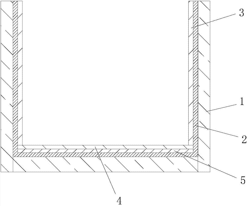
[0044] like figure 1 Shown, the present invention provides a kind of crucible, it comprises:

[0045] Crucible body 1;

[0046] The first coating 2, which is provided on the bottom wall and side wall of the crucible body 1, is used to prevent the metal impurities in the crucible body 1 from diffusing into the crystal located in the crucible body 1, affecting the quality of the crystal;

[0047] The second coating 3, which is arranged on the outside of the first coating 2 on the side wall, the second coating 3 is used to assist the nucleation of small grains on the side wall of the crucible body 1, so that the small grains on the side The defect density is low, and the extrusion force on the bottom columnar crystals is small, which provides better vertical growth conditions for the bottom columnar crystals; and


PUM

PropertyMeasurementUnit
particle diameteraaaaaaaaaa

Abstract

The invention provides a crucible and a preparation method thereof. The crucible comprises: a crucible body, a first coating, a second coating and a third coating, wherein the crucible body comprisesa bottom wall and a side wall; the first coating layer is arranged on the bottom wall and the side wall for preventing metal impurities from diffusing to crystalline grains in the crucible body, the second coating is arranged on the outside of the first coating layer on the side wall, the second coating layer is used to assist in nucleating the crystalline grains within the crucible body; the third coating is arranged on the outside of the first coating layer on the bottom wall, the third coating layer is used to assist in separating the crystalline grains within the crucible body from the crucible body. The crucible of the invention can effectively reduce diffusion of the metal impurities in the crucible body into polycrystalline crystals located in the crucible body, so that purity of the prepared polycrystalline silicon is high.

Description

technical field [0001] The invention relates to a crucible, in particular to a crucible for preparing polysilicon and a preparation method thereof. Background technique [0002] In recent years, with the depletion of non-renewable energy sources, solar cells have been developed rapidly. Since the preparation process of cast polysilicon is relatively simple and the cost is much lower than that of monocrystalline silicon, polysilicon gradually replaces the dominant position of Czochralski monocrystalline silicon in the solar cell material market and becomes the most important photovoltaic material in the industry. However, compared with Czochralski monocrystalline silicon, various defects in cast polycrystalline silicon, such as grain boundaries, dislocations, micro-defects, and impurity carbon and oxygen in the material, make the conversion efficiency of polycrystalline silicon solar cells lower than that of Czochralski monocrystalline silicon. Crystalline silicon solar cell...

Claims


Application Information

Patent Timeline
Patent Type & Authority Applications(China)
IPC IPC(8): C04B41/87C30B28/06C30B29/06
Inventor 常传波袁聪杨振帮唐骏
Owner YANGZHOU RONGDE NEW ENERGY TECH
Why Eureka
Try Eureka