
Silicon-based integrated tunable laser structure and control method thereof

A tunable laser, silicon-based technology, applied in the field of lasers, can solve the problems of low integration, unfavorable industrial processing and production, large volume, etc., and achieve the effects of high integration, high space utilization efficiency, and small volume

Active Publication Date: 2018-01-19
GUANGXUN SCI & TECH WUHAN
View PDF10 Cites 10 Cited by
  • Summary
  • Abstract
  • Description
  • Claims
  • Application Information

AI Technical Summary

Problems solved by technology

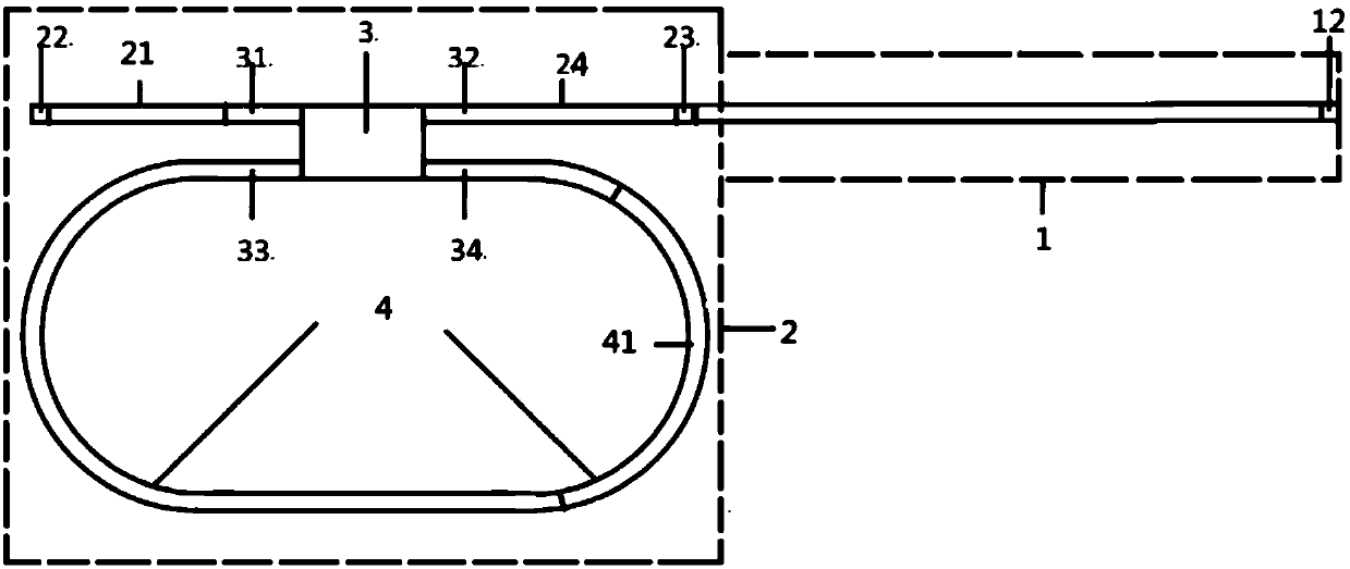
[0008] The technical problem to be solved by the present invention is that the silicon-based tunable laser in the prior art has a large volume and low integration; and, as figure 1 As shown, because of the optical path coupling involving the active resonator 1 and the passive mode selection cavity 2, the processing complexity of the silicon-based tunable laser is increased, which is not conducive to industrial processing and production

Method used


Image

  • Silicon-based integrated tunable laser structure and control method thereof
  • Silicon-based integrated tunable laser structure and control method thereof
  • Silicon-based integrated tunable laser structure and control method thereof

Examples


Embodiment 1

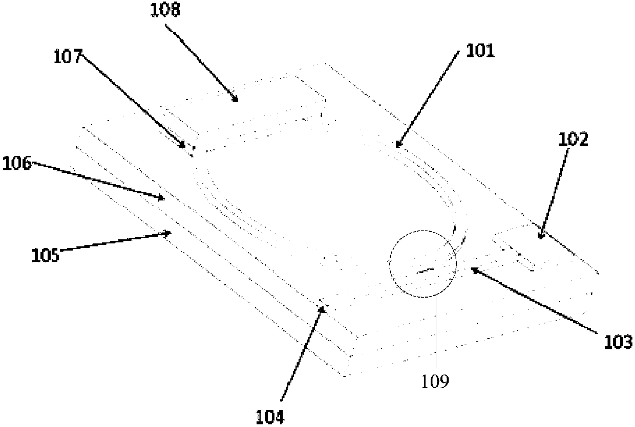
[0050] Embodiment 1 of the present invention provides a silicon-based integrated tunable laser structure, such as figure 2 As shown, it includes: a silicon-based microring resonator 101, a backlight detector 102, and a silicon-based coupling output waveguide 103 are fabricated on a silicon substrate 106. For example, the above-mentioned fabrication of a silicon-based A microring resonator 101 , a backlight detector 102 and a silicon-based outcoupling waveguide 103 . In an embodiment of the present invention, the tunable laser structure further includes:

[0051] The resonator 108 is bonded directly above the waveguide of the silicon-based microring resonator 101 through a polymer 107; image 3 As shown, where the optical signal generated by the active region of the resonator 108 is coupled into the silicon-based microring resonator 101 based on the evanescent wave, that is, the optical signal A generated by the active region in the figure is decomposed into an optical signal...

Embodiment 2

[0070] After providing a silicon-based integrated tunable laser structure as described in Embodiment 1, an embodiment of the present invention also provides a control method for a silicon-based integrated tunable laser structure, specifically, according to the method described in Embodiment 1 Si-based integrated tunable laser structures such as Figure 7As shown, the package is completed and the pins 403 (TEC+), 404 (TEC-), 405 (LD+), 406 (LD-), 407 (MPD+) and 408 (MPD- ), and lead out the output polarization maintaining fiber 409, wherein, the control chip 402 connects and controls one or more silicon-based integrated tunable laser packages, such as Figure 8 As shown, the control methods include:

[0071] In step 201, the control circuit 402 receives light from the i-th channel, and the center frequency of the light is λ set Optical power is P set The command.

[0072] In step 202, the control circuit 402 according to the λ set Set the voltage of the Nth channel TEC to ...


PUM


Abstract

The invention relates to the technical field of lasers, and provides a silicon-based integrated tunable laser structure and a control method thereof. A silicon-based micro-ring resonator, a backlightdetector and a silicon-based coupling output waveguide are manufactured on a silicon substrate. The resonator is bonded to be right above the waveguide of the silicon-based micro-ring resonator through a high-molecular polymer. A semiconductor refrigerator is arranged at the bottom of the silicon substrate and corresponds to the area wherein the silicon-based micro-ring resonator is located. An optical signal coupling structure is established below the waveguide of the silicon-based micro-ring resonator and at the middle region of the silicon-based coupling output waveguide. One end of the silicon-based coupling output waveguide is a light emitting surface. The other end of the silicon-based coupling output waveguide is coupled with the backlight detector. According to the invention, an active area is arranged above a silicon optical chip and the depth of the space is reasonably utilized. The space utilization efficiency is higher and the size of a manufactured optical device is smaller. The integration degree is high. The silicon-optical chip process is compatible with the CMOS process. Both the machinability and the yield are realized.

Description

【Technical field】 [0001] The invention relates to the technical field of lasers, in particular to a silicon-based integrated tunable laser structure and a control method thereof. 【Background technique】 [0002] Tunable lasers have been a research hotspot in the field of optical communication in recent years. [0003] The traditional light sources in the field of optical communication are all based on fixed-wavelength laser modules. With the continuous development and application of optical communication systems, the shortcomings of fixed-wavelength lasers are gradually revealed: on the one hand, with the development of DWDM technology, the number of wavelengths in the system There are hundreds of them. In the case where protection needs to be provided, the backup of each laser must be provided by a laser of the same wavelength, which leads to an increase in the number of backup lasers and an increase in cost; on the other hand, because fixed lasers need to distinguish wavele...

Claims


Application Information

Patent Timeline
Patent Type & Authority Applications(China)
IPC IPC(8): H01S5/10H01S5/187H01S5/30
Inventor 曹薇汤学胜胡毅马卫东
Owner GUANGXUN SCI & TECH WUHAN
Learn More