Electrostatic discharge protection circuit and manufacturing method thereof

A technology of electrostatic discharge protection and manufacturing method, which is applied in the direction of circuits, electrical components, electric solid devices, etc., can solve the problems of reducing the ESD protection ability of GGNMOS, uneven heat distribution, and reducing the service life of integrated circuits, so as to improve ESD protection effect of ability

Active Publication Date: 2020-11-27
SEMICON MFG INT (SHANGHAI) CORP +1
View PDF3 Cites 0 Cited by
  • Summary
  • Abstract
  • Description
  • Claims
  • Application Information

AI Technical Summary

Problems solved by technology

This inconsistent ESD turn-on phenomenon reduces the ESD protection capability of GGNMOS, and at the same time leads to uneven heat distribution in the GGMOS circuit, which can easily cause premature aging of the device and reduce the service life of the integrated circuit.

Method used


Image

  • Electrostatic discharge protection circuit and manufacturing method thereof
  • Electrostatic discharge protection circuit and manufacturing method thereof
  • Electrostatic discharge protection circuit and manufacturing method thereof

Examples


Embodiment 1

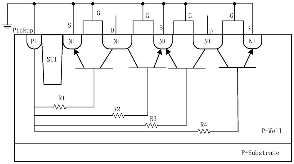
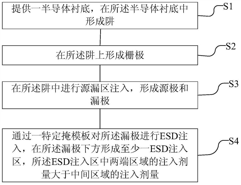
[0065] see Figure 2-Figure 7 , first, as figure 2 As shown, step S1 is performed to provide a semiconductor substrate, and a well is formed in the substrate. The selected semiconductor substrate in this embodiment is a P-type semiconductor substrate (P-Substrate), and the P-type semiconductor P-Well is formed in the substrate.

[0066] Then, execute step S2, such as Figure 4 As shown, a gate 13 is formed on the P-Well, and the formation of the gate 13 is polysilicon deposited by selective etching. The specific operation is to pass silane into the process chamber of the low-pressure chemical vapor deposition equipment, and the polysilicon generated by the decomposition of the silane is deposited on the surface of the P-Well. Then, in the photolithography area, the structure of the polysilicon gate is photoetched by deep ultraviolet lithography technology, and the polysilicon is etched by anisotropic plasma etching to form the gate 13 with a multi-finger structure.

[006...

Embodiment 2

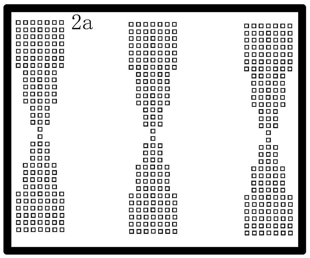
[0073] see Figure 8 , where reference numbers indicate the same Figure 2-Figure 7 The same expression and the same structure as the manufacturing method of the first embodiment. The manufacturing method of the second embodiment is basically the same as the manufacturing method of the first embodiment, the difference being that the specific mask used is different when ESD implantation is performed. In the second embodiment, at least one pair of funnel-shaped windows is provided on the specific mask plate 2b, each of the funnel-shaped windows has a large opening end and a small opening end, and each of the ESD injection regions corresponds to a pair of the The funnel-shaped window, in each pair of the funnel-shaped window, the small opening ends are oppositely arranged and correspond to the middle area of ​​the ESD injection region, and the large opening ends are arranged opposite to each other and correspond to the two sides of the ESD injection region end area. Refer to E...


PUM


Abstract

The invention discloses an electrostatic discharge protection circuit and a manufacture method thereof. The manufacture method of the electrostatic discharge protection circuit includes the followingsteps that: a semiconductor substrate is provided, a well is formed in the semiconductor substrate; a gate is formed on the well; source and drain region implantation is performed in the well, so thatsource electrodes and drain electrodes are formed; and ESD (electrostatic discharge protection) implantation is performed on the drain electrodes through a specific mask, so that ESD implantation regions can be formed under the drain electrodes, the implantation dose of two end regions in each ESD implantation region is greater than that of a middle region in the corresponding ESD implantation region. According to the electrostatic discharge protection circuit and the manufacture method thereof of the invention, ESD implantation is performed through the specific mask, so that at least one ESDimplantation region is formed under the drain electrode; the implantation dose of the two end regions in the ESD implantation region is greater than that of the middle region in the ESD implantationregion; and therefore, the problem of inconsistency of the start of ESD in an existing electrostatic discharge protection circuit can be solved, and the electrostatic discharge protection capability of the electrostatic discharge protection circuit of the invention can be effectively improved.

Description

technical field [0001] The invention relates to the field of semiconductor manufacturing, in particular to an electrostatic discharge protection circuit and a manufacturing method thereof. Background technique [0002] Integrated circuits are easily damaged by static electricity. Generally, an electrostatic protection circuit is designed in the input and output terminals of the circuit or in the power protection device to prevent the internal circuit from being damaged by static electricity. At present, GGNMOS (Gate Grounded NMOS, gate grounded N-type metal oxide semiconductor) is often used as an electrostatic discharge protection circuit. [0003] However, there are still some defects in the existing GGNMOS circuits, such as figure 1 As shown, it is a schematic cross-sectional view of the structure of the existing GGNMOS. A well (P-Well) is formed on the substrate (P-Substrate). In the NMOS region of the GGNMOS, the source S and the gate G are grounded, and the pickup reg...

Claims


Application Information

Patent Timeline
Patent Type & Authority Patents(China)
IPC IPC(8): H01L27/02
Inventor 甘正浩
Owner SEMICON MFG INT (SHANGHAI) CORP
Why Eureka
Try Eureka