Graphene-niobium selenide superconducting heterojunction device and preparation method thereof
A graphene, niobium selenide technology, applied in superconducting devices, semiconductor devices, electrical components, etc., can solve the problems of weak van der Waals force binding, difficult product size, easy introduction of impurities, etc., to achieve product size control, product size Easy, simple craftsmanship
- Summary
- Abstract
- Description
- Claims
- Application Information
AI Technical Summary
Problems solved by technology
Method used
Image
Examples
Embodiment 1
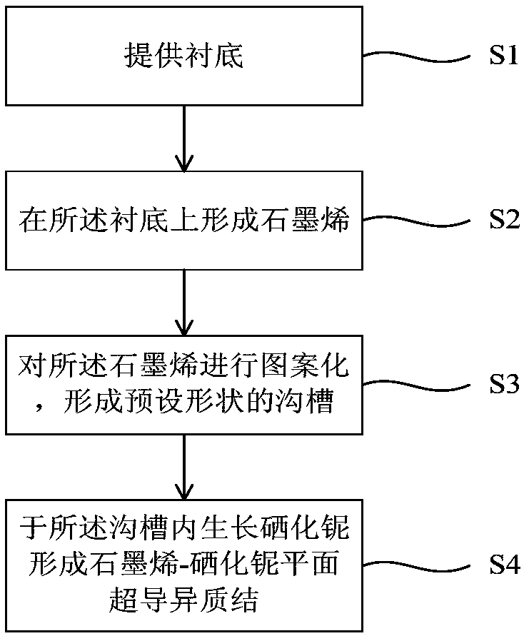
[0048] Such as figure 1 As shown, it shows a schematic diagram of the preparation process of the graphene-niobium selenide superconducting heterojunction device of the present invention. The preparation method of the graphene-niobium selenide superconducting heterojunction device of the present embodiment includes the following steps:
[0049] Step S1, providing a substrate 1, such as figure 2 shown. As an example, the substrate 1 may be one of silicon, silicon oxide, glass, ceramic and polymer or a composite material of two or more. In this embodiment, a silicon material with silicon oxide attached to its surface is used as the substrate 1, wherein the silicon oxide is an insulating layer.
[0050] Step S2, forming graphene 2 on the upper surface of the substrate 1, such as image 3 shown.
[0051] Specifically, the specific method of step S2 may include: directly forming the graphene 2 on the substrate 1 by mechanical exfoliation, or transferring the graphene 2 to the s...
Embodiment 2
[0075] In the first embodiment, the number of the trench 3 is 1, and the graphene 2 is divided into two independent regions. However, in this embodiment, the number of the grooves 3 is two, and the graphene 2 is divided into three independent regions. Such as Figure 7 As shown, it is a schematic structural diagram of a graphene-niobium selenide superconducting heterojunction device. The preparation method of the graphene-niobium selenide superconducting heterojunction device in this embodiment includes the following steps:
[0076] In step S1 , a substrate 1 is provided. As an example, the substrate 1 may be one of silicon, silicon oxide, glass, ceramic and polymer or a composite material of two or more. In this embodiment, a silicon material with silicon oxide attached to its surface is used as the substrate 1, wherein the silicon oxide is an insulating layer.
[0077] Step S2, forming graphene 2 on the upper surface of the substrate 1, such as image 3 shown.
[0078] S...
Embodiment 3
[0102] The present invention also provides a graphene-niobium selenide planar heterojunction device, please refer to Figure 7 , the graphene-niobium selenide superconducting heterojunction device includes a substrate 1 , graphene 2 , trench 3 , and niobium selenide 4 .
[0103] Specifically, the graphene 2 is located above the substrate 1 .
[0104] Specifically, the groove 3 is located in the graphene 2, and the graphene 2 is patterned to form the graphene 2 with a predetermined shape. In this embodiment, the number of the grooves 3 is two.
[0105] Specifically, the niobium selenide 4 is located in the trench 3, and the niobium selenide is connected to the edge of the graphene 2 to form a graphene-niobium selenide planar superconducting heterojunction.
[0106] Specifically, the groove 3 is straight, curved, or a combination of one or both of the straight and curved. In this embodiment, the groove 3 is rectangular.
[0107] The graphene-niobium selenide planar supercond...
PUM
 Abstract
Description
Claims
Application Information
 - R&D
- Intellectual Property
- Life Sciences
- Materials
- Tech Scout
- Unparalleled Data Quality
- Higher Quality Content
- 60% Fewer Hallucinations
Browse by: Latest US Patents, China's latest patents, Technical Efficacy Thesaurus, Application Domain, Technology Topic, Popular Technical Reports.
© 2025 PatSnap. All rights reserved.Legal|Privacy policy|Modern Slavery Act Transparency Statement|Sitemap|About US| Contact US: help@patsnap.com


