Two-dimensional black phosphorus pn junction, its preparation method and application

A PN junction and black phosphorus technology, applied in semiconductor devices, electrical components, circuits, etc., can solve the problems of complex process, low yield, and low efficiency, and achieve the effect of good repeatability and simple and efficient preparation method

Active Publication Date: 2021-02-26
SUZHOU INST OF NANO TECH & NANO BIONICS CHINESE ACEDEMY OF SCI
View PDF1 Cites 0 Cited by
  • Summary
  • Abstract
  • Description
  • Claims
  • Application Information

AI Technical Summary

Problems solved by technology

For example, some researchers prepared black phosphorus-MoS 2 heterojunction, the method requires exfoliation-transferred MoS 2 , also need to use self-alignment technology, the process is more complicated, and the yield is low
Another researcher used the double back gate structure to prepare black phosphorus PN junction, but this method also needs to use self-alignment technology, so the efficiency is low

Method used


Image

  • Two-dimensional black phosphorus pn junction, its preparation method and application
  • Two-dimensional black phosphorus pn junction, its preparation method and application
  • Two-dimensional black phosphorus pn junction, its preparation method and application

Examples


preparation example Construction

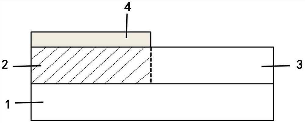
[0035] The embodiment of the present invention also provides a method for preparing a two-dimensional black phosphorus PN junction, which includes:

[0036] Provide two-dimensional black phosphorus film;

[0037] Perform n-type doping to a local area of ​​the black phosphorus film to form an n-type semiconductor, while keeping other local areas of the black phosphorus film as a p-type semiconductor, and make the n-type semiconductor cooperate with the p-type semiconductor to form a PN semiconductor. Knot.

[0038] In some embodiments, the preparation method includes: at least selecting a physical and / or chemical deposition method to deposit a film with charge transfer doping properties on a local area of ​​the black phosphorus film surface, so that the local black phosphorus film The region is n-type doped to form an n-type semiconductor.

[0039] Furthermore, the constituent substances of the film with charge-transfer doping properties deposited on the surface of the black ...

Embodiment 1

[0049] Example 1: A black phosphorus film with a thickness of 5 to 20 nanometers is obtained by exfoliating black phosphorus crystals using a micromechanical exfoliation method or a liquid phase exfoliation method, and transferring the black phosphorus film to a substrate, which includes but is not limited to Silicon wafer, quartz, silicon oxide, silicon carbide, aluminum oxide, PET, etc. Further, a layer of Si is deposited on the local surface of the black phosphorus film x N y Thin film, the deposition method includes PECVD, ICPCVD, LPCVD or thermal evaporation, etc., the silicon source gas used in the deposition method includes SiN 4 、SiF 4 、SiCl 3 H, SiCl 4 、SiH 2 Cl 2 Any one or a combination of two or more of them, but not limited thereto. The nitrogen source gas used in the deposition method includes N 2 O, N 2 , NH 3 Any one or a combination of two or more of them, but not limited thereto. Further, the volume ratio of silicon source gas to nitrogen source ga...

Embodiment 2

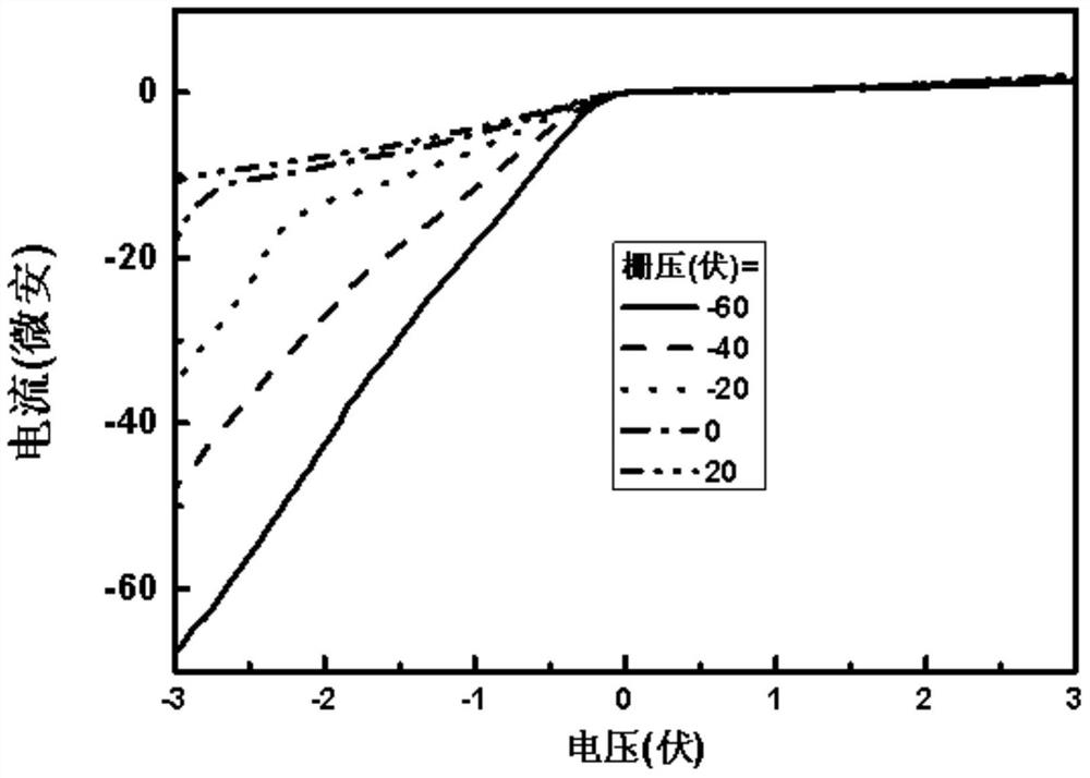
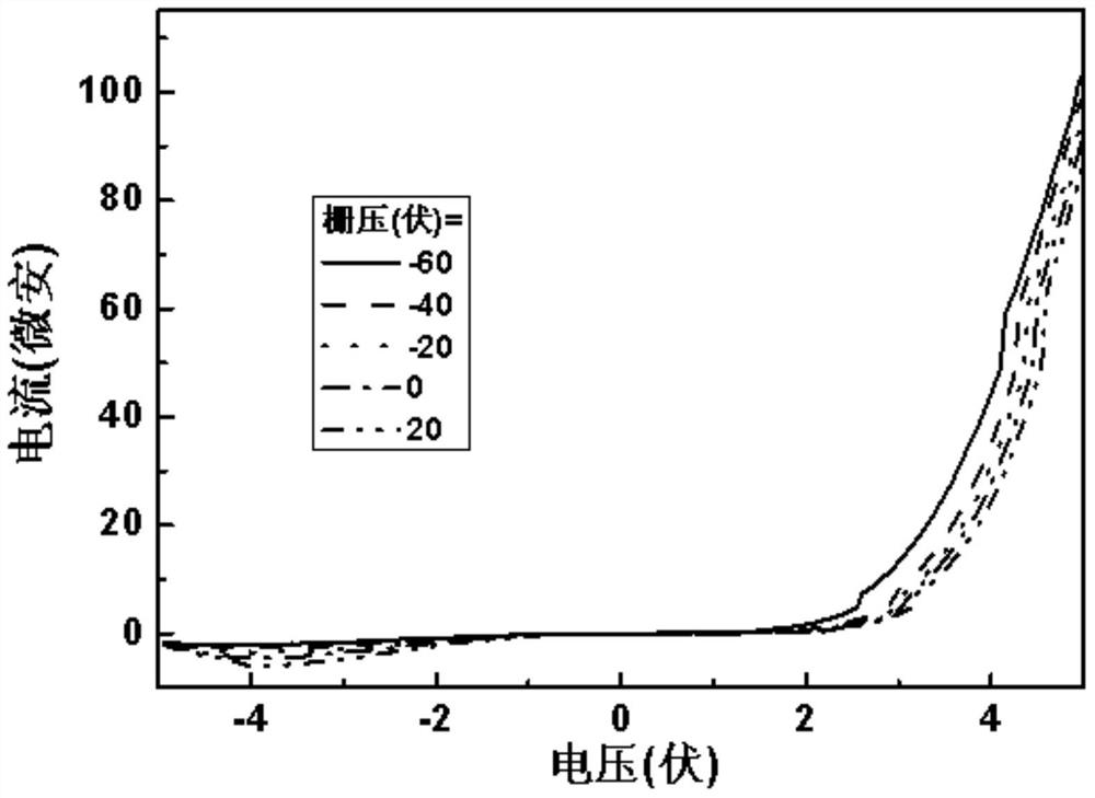
[0054] Embodiment 2: Use the micromechanical stripping method or the liquid phase stripping method to obtain a black phosphorus film with a thickness of 40 to 60 nanometers from the black phosphorus crystal, transfer the film to a silicon substrate, and then use the method of spin coating on the black phosphorus surface A layer of 1,5-naphthalene diamine thin film is deposited in a local area, and the film thickness is 1000-2000 nanometers. It is found by testing the electrical properties that the two-dimensional black phosphorus PN junction samples obtained in this embodiment also have obvious unidirectional conductivity. For example, the test results of a typical black phosphorus PN junction sample can be found in image 3 . These black phosphorus PN junctions are suitable for making rectifier diodes.


PUM

PropertyMeasurementUnit
thicknessaaaaaaaaaa
thicknessaaaaaaaaaa
thicknessaaaaaaaaaa

Abstract

The invention discloses a two-dimensional black phosphorus PN junction, which may include a two-dimensional black phosphorus film, at least a partial area of ​​the surface of the black phosphorus film is covered with a film with charge transfer characteristics; and at least on the black phosphorus film At the joint interface with the film with charge transfer properties, the black phosphorus film is doped by the constituent substances of the film with charge transfer doping properties to form an n-type semiconductor; at the same time, the black phosphorus film also contains p-type semiconductor Black phosphorus; the n-type semiconductor is combined with the p-type semiconductor to form a PN junction. The invention also discloses a preparation method of the two-dimensional black phosphorus PN junction. The black phosphorus PN junction provided by the invention has properties such as unidirectional conductivity and photovoltaic special effect, and is suitable for preparing micro-nano devices such as rectifier diodes, switching diodes, and photovoltaic cells. The semiconductor process is compatible, which is of positive significance to the wide application of black phosphorus in many fields.

Description

technical field [0001] The invention relates to a method for preparing a two-dimensional semiconductor PN junction, in particular to a two-dimensional black phosphorus PN junction, its preparation method and applications, such as applications in rectifier diodes, switching diodes, photodetectors, and photovoltaic cells. Background technique [0002] Since graphene was first discovered in 2004, two-dimensional materials have received extensive research boom because of their unique properties. Graphene has excellent mechanical, electrical, optical, thermal and other properties, and has great application potential in many fields such as transparent conductive electrodes, supercapacitors, flexible devices, and batteries. But the disadvantage of graphene is that it has no band gap, so it cannot be used in logic circuits. Transition metal dichalcogenides (TMDs) such as MoS 2 、WS 2 Other two-dimensional materials have a band gap, but the band gap range is narrow (1.2-1.8eV), whi...

Claims


Application Information

Patent Timeline
Patent Type & Authority Patents(China)
IPC IPC(8): H01L29/24
Inventor 张跃钢张凯徐轶君
Owner SUZHOU INST OF NANO TECH & NANO BIONICS CHINESE ACEDEMY OF SCI
Why Eureka
Try Eureka