A palladium-doped carbon thin film material with photovoltaic effect

A photovoltaic effect, carbon thin film technology, applied in photovoltaic power generation, sustainable manufacturing/processing, electrical components, etc., can solve the problem that single-walled carbon nanotubes are expensive and limit the application of single-walled carbon nanotubes/silicon heterojunction solar cells and development and other issues, to achieve the effect of abundant reserves, good application value and low price

Inactive Publication Date: 2011-12-21
CHINA UNIV OF PETROLEUM (EAST CHINA)
View PDF2 Cites 0 Cited by
  • Summary
  • Abstract
  • Description
  • Claims
  • Application Information

AI Technical Summary

Problems solved by technology

However, single-walled carbon nanotubes are expensive, which limits the application and development of single-walled carbon nanotubes / silicon heterojunction solar cells.

Method used


Image

  • A palladium-doped carbon thin film material with photovoltaic effect
  • A palladium-doped carbon thin film material with photovoltaic effect
  • A palladium-doped carbon thin film material with photovoltaic effect

Examples


Embodiment 1

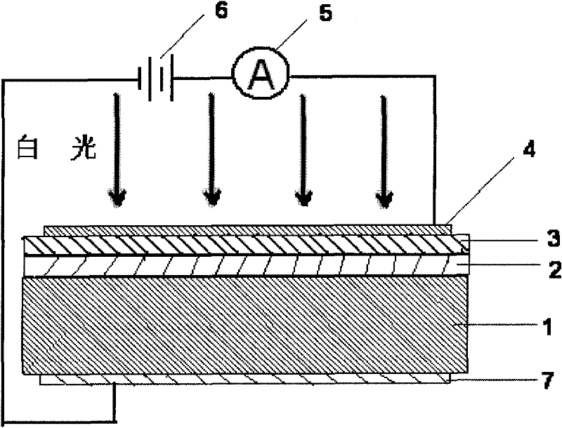
[0024] Example 1, take graphite powder with a purity of 99.9%, mix it with palladium powder with a purity of 99.9%, and make a palladium-carbon composite target with a palladium atomic number content of 1% by cold pressing. The palladium-carbon composite target is sputtered onto a silicon wafer 1 with a thickness of 1.0 mm to retain a natural oxide layer 2 by magnetron sputtering. The thickness of silicon dioxide 2 is about 1.2 nanometers, forming a silicon wafer on the silicon wafer. A palladium-doped carbon film 3 with a layer thickness of 100 nanometers is sputtered with a semi-transparent copper film 4 on the palladium-doped carbon film 3, the copper film 4 is used as an upper electrode, and 7 is an indium back electrode. Connect the DC power supply 6 on the semiconductor-oxide-semiconductor (SIS) structure material, and the ammeter 5 becomes an SIS structure with photovoltaic effect, such as figure 1 shown. The sputtering DC voltage was 0.40 kV, the sputtering DC current...

Embodiment 2

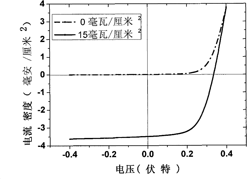
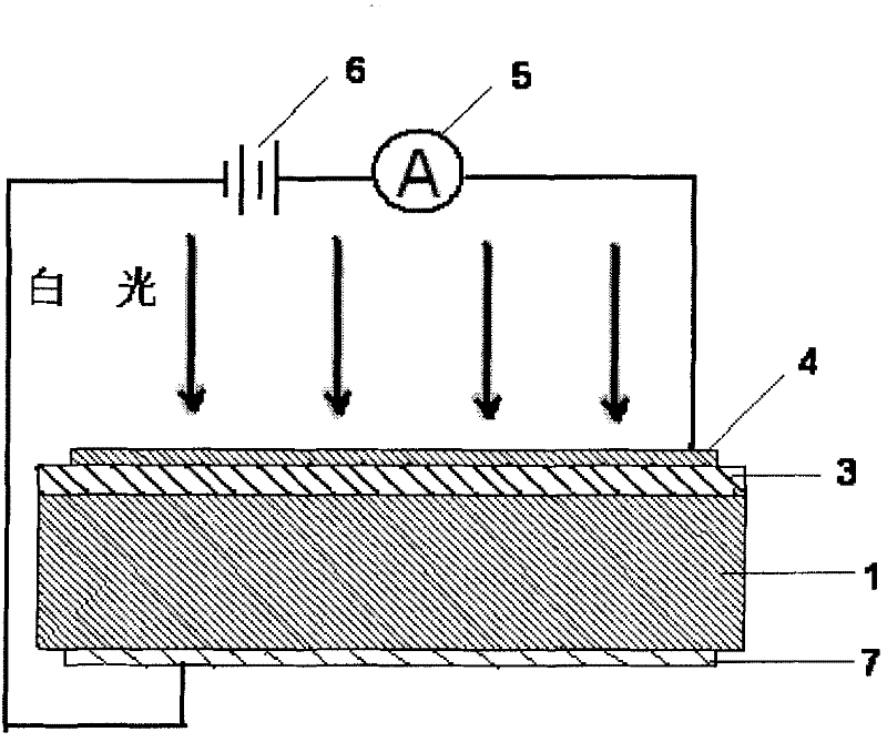
[0025] Example 2, take graphite powder with a purity of 99.9%, mix it with palladium powder with a purity of 99.9%, and make a palladium-carbon composite target with a palladium atomic number content of 2% by cold pressing. The palladium-carbon composite target is sputtered onto a silicon wafer 1 with a thickness of 1.0 mm by magnetron sputtering, and a palladium-doped carbon film 3 with a thickness of 100 nanometers is formed on the silicon wafer. 3 is sputtered with a layer of translucent copper film 4, the copper film 4 is used as an upper electrode, and 7 is an indium back electrode. Connect the DC power supply 6 on the heterojunction material, and the ammeter 5 becomes a heterojunction with photovoltaic effect, such as image 3shown. The sputtering DC voltage was 0.40 kV, the sputtering DC current was 0.12 A, the sputtering deposition temperature was 350° C., and the sputtering time was 90 minutes. mW / cm on sample at room temperature 2 The current density-voltage chara...


PUM

PropertyMeasurementUnit
thicknessaaaaaaaaaa
thicknessaaaaaaaaaa
electric potential / voltageaaaaaaaaaa

Abstract

The invention provides a palladium-doped carbon film material with photovoltaic effect. A film with the thickness of 20-200nm is sputtered on a 0.5-1.0mm mono-crystalline silicon wafer to manufacture a palladium-doped carbon film / silicon dioxide / silicon material or palladium-doped carbon film / silicon heterogenous junction material, wherein the film with the thickness of 20-200nm is a carbon film with the doped palladium atom content of 0-5%. The material has photovoltaic effect, and can be used for manufacturing solar cells and photosensitive devices; and the manufactured solar cells have higher conversion efficiency, and have simple manufacture process and high finished product ratio.

Description

technical field [0001] The invention relates to a material with photovoltaic effect, which is used to manufacture solar cells and photosensitive sensor devices. Background technique [0002] In 1954, Bell Laboratories Chapin et al. developed the first pn junction silicon solar cell. Since then, people have conducted extensive research on inorganic solar cells. [0003] Today, the tense global energy situation and climate warming caused by carbon dioxide emissions have seriously threatened economic development and people's normal life. Therefore, all countries in the world are actively seeking new energy sources to replace traditional energy sources such as oil and coal, so as to achieve sustainable development and gain an advantageous position in future development. Solar energy has become the focus of attention due to its obvious advantages such as cleanliness, pollution-free, and safety. Moreover, solar energy is a truly inexhaustible and inexhaustible source of energy. ...

Claims


Application Information

Patent Timeline
Patent Type & Authority Patents(China)
IPC IPC(8): H01L31/0288H01L31/042H01L31/18
CPCY02E10/50Y02P70/50
Inventor 薛庆忠马明陈惠娟吕成夏丹
Owner CHINA UNIV OF PETROLEUM (EAST CHINA)
Why Eureka
Try Eureka