WSe2 thin sheet/In2O3 nanowire composite-structure near-infrared photoelectric detector and fabrication method thereof
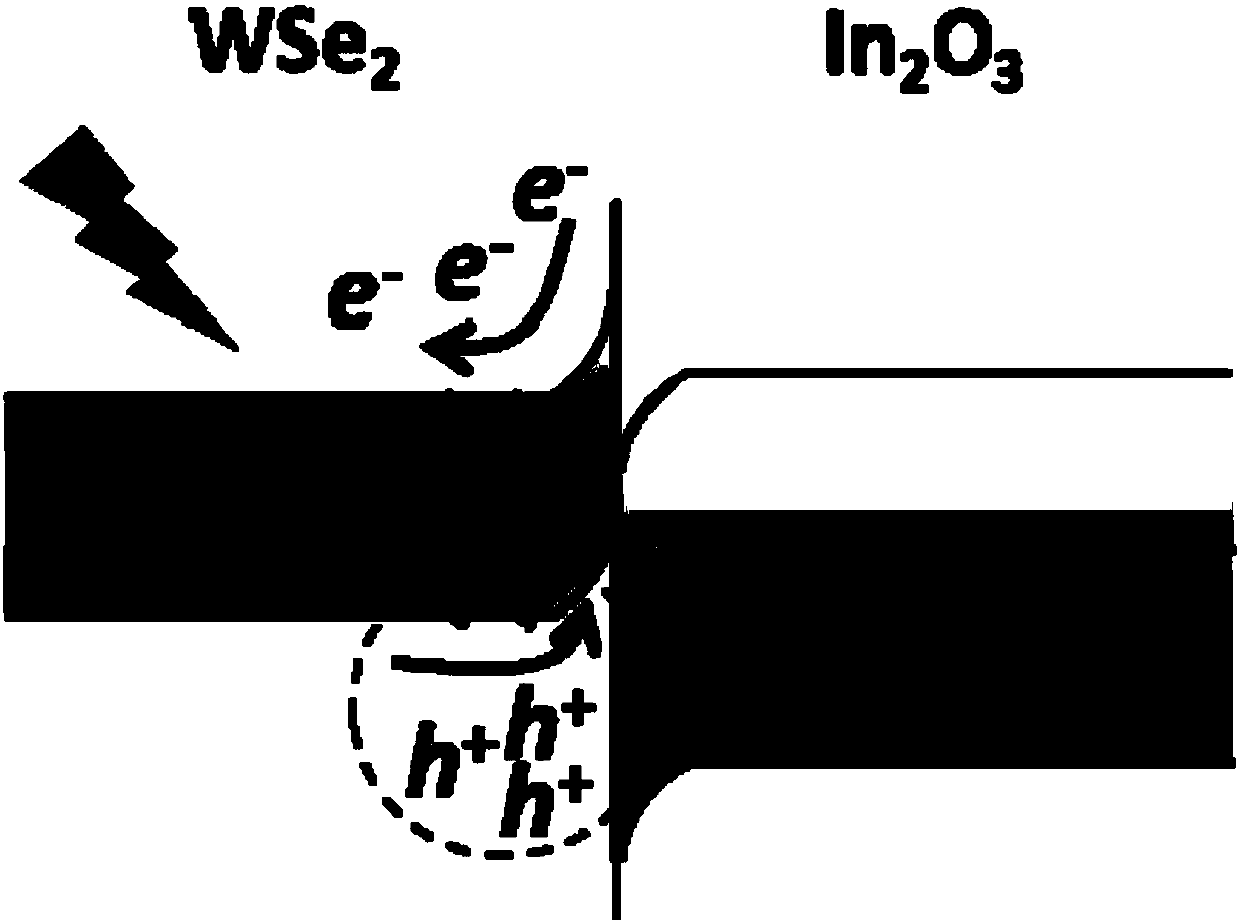
A tungsten diselenide, near-infrared light technology, applied in circuits, electrical components, semiconductor devices, etc., can solve the problems of low light utilization efficiency, inhibit the photoresponsivity and detection rate of devices, and achieve high response and high detection rate. Effect
- Summary
- Abstract
- Description
- Claims
- Application Information
AI Technical Summary
Problems solved by technology
Method used
Image

Examples
preparation example Construction
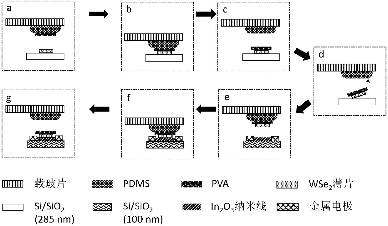
[0031] Such as figure 2 As shown, a preparation method of a tungsten diselenide flake / indium oxide nanowire composite structure near-infrared photodetector, the steps of the method include:
[0032] (1) Growth of In by chemical vapor deposition 2 o 3 Nanowires;
[0033] (2) In the preparation of step (1) 2 o 3 Physical transfer of nanowires to Si / SiO 2 (100nm) on the substrate;
[0034] (3) Using electron beam lithography technology and thermal evaporation metal electrode to prepare single In 2 o 3 Nanowire back-gate transistor devices;
[0035] (4) Using the method of mechanical exfoliation on Si / SiO 2 Preparation of WSe on (285nm) Substrate 2 nanosheets;
[0036] (5) WSe prepared by step (4) 2 The nanoflakes are transferred to the In prepared in step (3) 2 o 3 A composite structure of tungsten diselenide flake / indium oxide nanowire is obtained on the back gate transistor device of the nanowire.
[0037] In the described step (5), the WSe 2 The nanoflakes tra...
Embodiment
[0041] (1) Growth of In by chemical vapor deposition 2 o 3 nanowires and their physical transfer to Si / SiO 2 (100nm) substrate, the source-drain (S-D) metal electrode Cr / Au (15nm / 50nm) was deposited by electron beam lithography technology and thermal evaporation technology to prepare a single In 2 o 3 Nanowire back gate transistor device, heavily doped p-type Si substrate as back gate electrode;
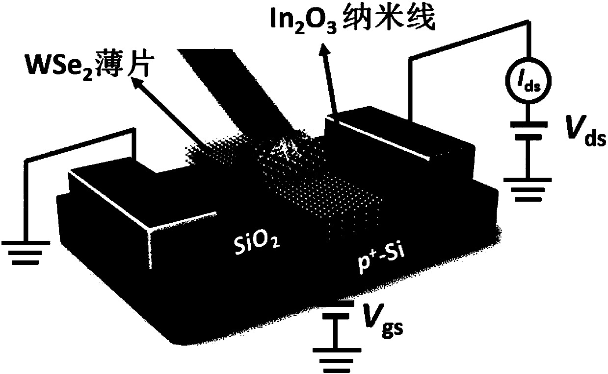
[0042] (2) Using the method of mechanical exfoliation on Si / SiO 2 Preparation of WSe on (285nm) Substrate 2 nanoflakes, due to the two-dimensional material WSe 2 As the number of layers increases from single layer to multilayer, the bandgap width decreases from 1.7eV to 1.2eV, so in order to respond to the near-infrared band, choose thick WSe with narrower bandgap 2 nanoflakes, and the WSe 2 flakes transferred to In 2 o 3 On the back-gate transistor devices of nanowires, composite structures such as figure 1 shown, the source-drain bias is V ds , the back gate bias is V g...
PUM
| Property | Measurement | Unit |
|---|---|---|
| Thickness | aaaaa | aaaaa |
| Thickness | aaaaa | aaaaa |
Abstract
Description
Claims
Application Information
 - R&D Engineer
- R&D Manager
- IP Professional
- Industry Leading Data Capabilities
- Powerful AI technology
- Patent DNA Extraction
Browse by: Latest US Patents, China's latest patents, Technical Efficacy Thesaurus, Application Domain, Technology Topic.
© 2024 PatSnap. All rights reserved.Legal|Privacy policy|Modern Slavery Act Transparency Statement|Sitemap