Method for manufacturing thin-film resistor through ICP dry etching

A thin-film resistor and dry etching technology, which is applied in the direction of resistors, circuits, electrical components, etc., can solve the problems of slow etching rate, poor controllability of key dimensions, and difficult control of substrate damage, and achieve the effect of ensuring stability

Active Publication Date: 2018-02-27
CHONGQING ZHONGKE YUXIN ELECTRONICS
View PDF7 Cites 6 Cited by
  • Summary
  • Abstract
  • Description
  • Claims
  • Application Information

AI Technical Summary

Problems solved by technology

[0003] CRSI usually adopts wet etching process, but wet etching has poor control over key dimensions, which limits the application of CrSi thin films
The US patent US20110086488AL granted to Abbas ALI et al. discloses a method using Cl2 and O 2 The method of etching thin films such as SICR, SICRC, SICRCO, and CRON adopts the reactive ion etching (RIE) process, and the etching rate is relatively slow (34nm SICRC is etched within 60 seconds, and the reaction rate is 0.57nm / Sec). Substrate damage control is difficult

Method used


Image

  • Method for manufacturing thin-film resistor through ICP dry etching
  • Method for manufacturing thin-film resistor through ICP dry etching
  • Method for manufacturing thin-film resistor through ICP dry etching

Examples


Embodiment 1

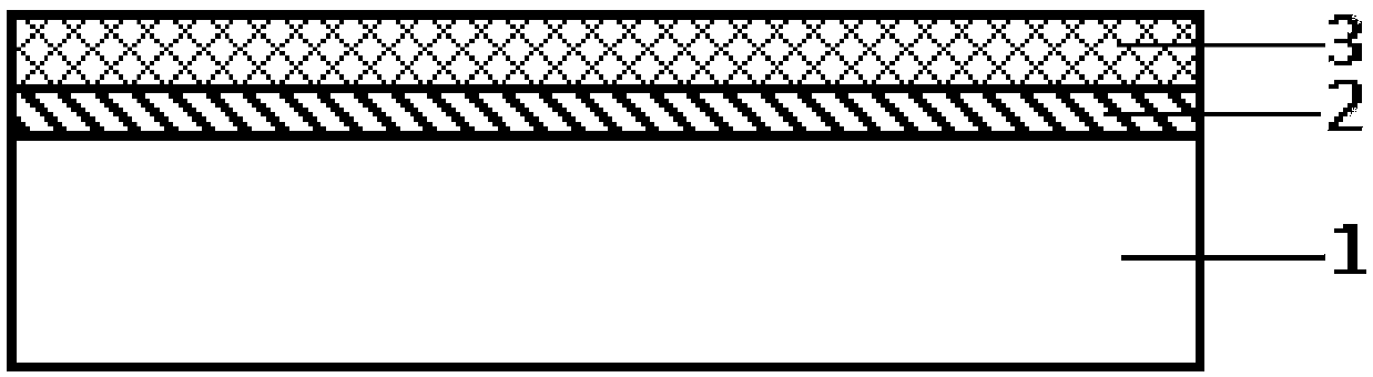
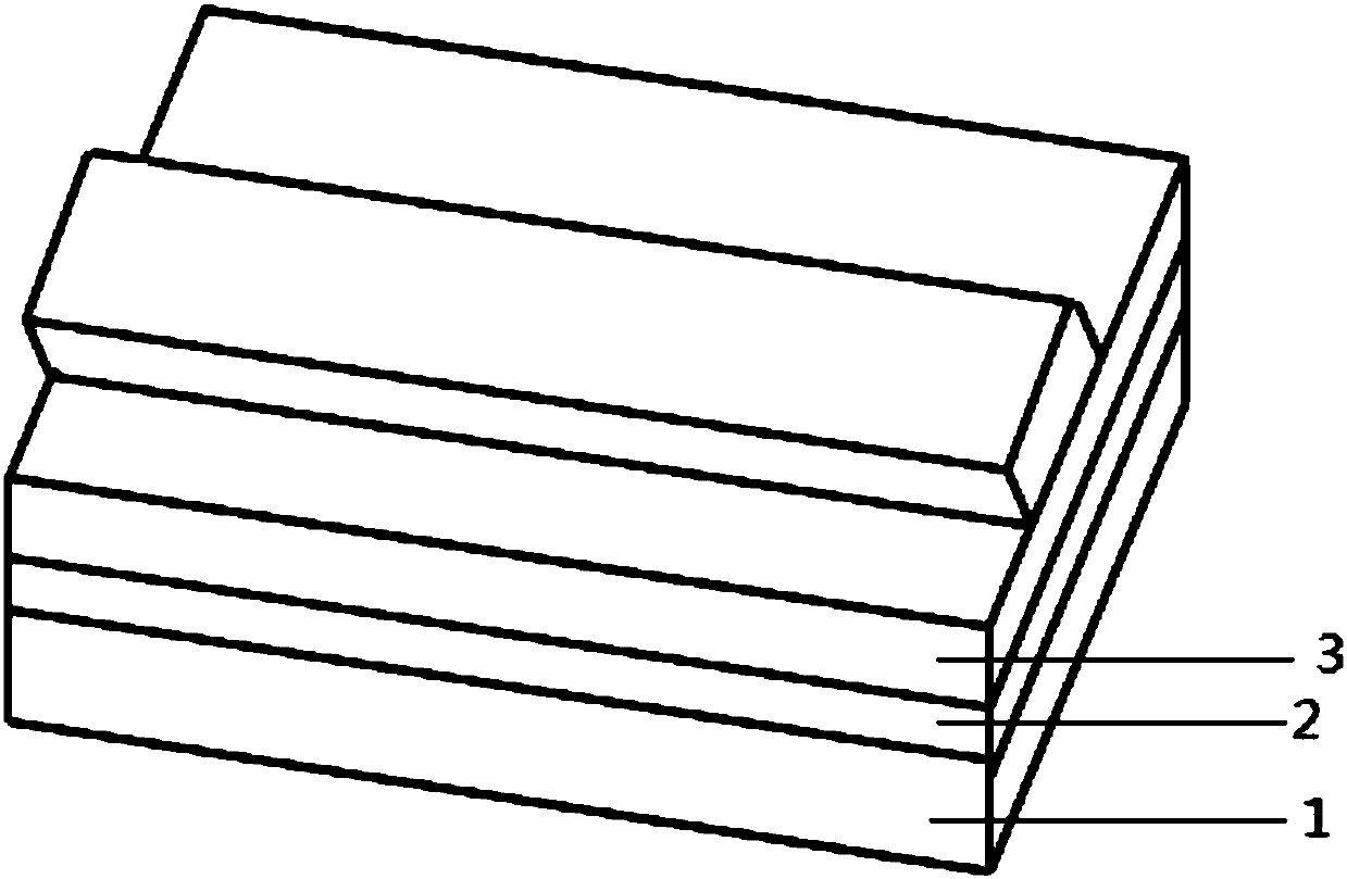
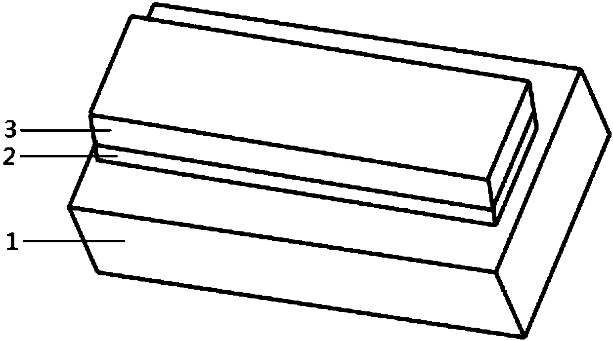
[0039] A method for manufacturing thin-film resistors by ICP dry etching, which is characterized by comprising: a substrate dielectric layer 1, a thin-film resistor layer 2, a mask layer 3, a dielectric layer 4, an isolation layer 5 and a metal layer 6.

[0040] Do the following steps:

[0041] 1) Deposit a resistive thin film layer 2 on the substrate dielectric layer 1 .

[0042] The resistive film layer 2 in the step 1) is a metal film containing Cr, including CrSi.

[0043] 2) Depositing a masking layer 3 on the resistive thin film layer 2 .

[0044] The masking layer 3 in the step 2) is a material with a high selectivity ratio, and the masking layer 3 includes Ti or Tin.

[0045] The selection ratio of the material of the resistive film layer 2 and the material of the masking layer 3 is greater than or equal to 6.

[0046] 3) Removing the resistive thin film layer 2 and the masking layer 3 by ICP dry etching to form a resistive pattern.

[0047] In the step 3), ICP pla...

Embodiment 2

[0057] A method for manufacturing thin-film resistors by ICP dry etching, which is characterized by comprising: a substrate dielectric layer 1, a thin-film resistor layer 2, a mask layer 3, a dielectric layer 4, an isolation layer 5 and a metal layer 6.

[0058] Do the following steps:

[0059] 1) if figure 1 As shown, a resistive thin film layer 2 is deposited on the substrate dielectric layer 1 .

[0060] The substrate dielectric layer 1 is an insulating medium;

[0061] The resistance film layer 2 is CrSi, and the thickness of the resistance film layer 2 is 45±5nm;

[0062] 2) if figure 1 A masking layer 3 is deposited on the resistive film layer 2 as shown.

[0063] The masking layer 3 in the step 2) is a material with a high selectivity ratio, and the masking layer 3 includes Ti or Tin; the thickness of the masking layer 3 is about 10±1 nm.

[0064] The selection ratio of the material of the resistive film layer 2 and the material of the masking layer 3 is greater than...

Embodiment 3

[0082] In this embodiment, the specific parameters for etching the CRSI metal layer by ICP are shown in Table 1:

[0083] Table 1

[0084]

[0085]

[0086] specific:

[0087] Utilize the OMEGA machine platform of TRIKON Company in the present invention, adopt the mode of two-step etching:

[0088] In the first step, the etching gas used is Cl 2 , HBr and Ar, and through the way of endpoint detection, used to etch most metals;

[0089] In the present invention, the first etching step adopts Cl 2 , the flow rate of HBr and Ar can be adjusted according to the composition of the metal film and the etching requirements, where Cl 2 As the main etching gas, Ar mainly provides physical bombardment; HBr is used for auxiliary etching and sidewall protection;

[0090] In the first step of etching, the etching end point is detected by means of end point detection. In this embodiment, the 55±6nm masking layer / CRSI film reaches the end point within 12-18 sec, and the etching rat...


PUM


Abstract

The invention discloses a method for manufacturing a thin-film resistor through ICP dry etching. The method is characterized in that a substrate dielectric layer, a thin-film resistor layer, a maskinglayer, a dielectric layer, an isolating layer and a metal layer are involved. The method includes the following steps that 1, the thin-film resistor layer is deposited on the substrate dielectric layer; 2, the masking layer is deposited on the thin-film resistor layer; 3, the thin-film resistor layer and the masking layer are removed through ICP dry etching, and a resistor pattern is formed; 4, the dielectric layer is deposited on the resistor pattern, the redundant part of the dielectric layer is removed through a photoetching process, and the ends of the dielectric layer are retained; 5, the redundant part of the masking layer on the thin-film resistor layer is removed through an etching process, and the parts, protected by the ends of the dielectric layer, of the masking layer are retained; 6, the isolating layer is deposited on the resistor pattern, and connecting holes are formed in the resistor ends through etching; 7, the metal layer is deposited, the connecting holes are filled, and the resistor is led out.

Description

technical field [0001] The invention relates to the field of semiconductor integrated circuits, in particular to a method for manufacturing thin-film resistors by ICP dry etching. Background technique [0002] Compared with diffusion resistance and injection resistance, CRSI thin film resistance has the advantages of lower temperature coefficient, smaller parasitic parameters and wider resistance range, so it has become the basis of precision resistance network for high-precision integrated circuits and module circuits. With the further development of integrated circuits in the direction of high precision and high stability, higher requirements are put forward for the preparation process of CRSI thin film resistors that form precision resistor networks. [0003] CRSI usually uses a wet etching process, but wet etching has poor control over critical dimensions, which limits the application of CrSi thin films. The US patent US20110086488AL granted to Abbas ALI et al. disclose...

Claims


Application Information

Patent Timeline
Patent Type & Authority Applications(China)
IPC IPC(8): H01L21/306H01L21/308H01L23/64
CPCH01L21/3065H01L21/308H01L28/20
Inventor 郭亿文冉明王学毅王飞崔伟
Owner CHONGQING ZHONGKE YUXIN ELECTRONICS
Why Eureka
Try Eureka