
Back contact heterojunction solar cell with by low laser damage as characteristic, and and manufacturing method thereof

A technology for solar cells and manufacturing methods, applied in photovoltaic power generation, final product manufacturing, sustainable manufacturing/processing, etc., can solve problems such as sensitivity to laser thermal effects, and achieve the effects of controlling laser damage, decreasing aperture ratio, and reducing processes

Pending Publication Date: 2022-02-18
福建金石能源有限公司
View PDF0 Cites 2 Cited by
  • Summary
  • Abstract
  • Description
  • Claims
  • Application Information

AI Technical Summary

Problems solved by technology

However, since the amorphous silicon-based heterojunction itself is a low-temperature process (less than 200 degrees), the grown film layer is more sensitive to the thermal effect of the laser. How to reduce the thermal attenuation effect caused by the laser opening is the responsibility of the back contact technology. One of the important research and development topics

Method used


Image

  • Back contact heterojunction solar cell with by low laser damage as characteristic, and and manufacturing method thereof
  • Back contact heterojunction solar cell with by low laser damage as characteristic, and and manufacturing method thereof
  • Back contact heterojunction solar cell with by low laser damage as characteristic, and and manufacturing method thereof

Examples


preparation example Construction

[0068] The preparation process of the hydrogen-doped indium oxide thin film is to use pure indium oxide as a target material, then introduce hydrogen or water vapor into the process gas, and form a hydrogen-doped indium oxide thin film by physical vapor deposition.

[0069] The specific method of the step F is to print the anti-plating ink on the conductive layer obtained through the step E treatment.

[0070] The specific method of the step G is to prepare the first conductive region electrode and the second conductive region electrode by electroplating on the first conductive region and the second conductive region treated in the step C.

[0071] The specific process of step G is to form an electroplated copper grid electrode by immersion or horizontal brush contact, and form a protective tin of 100 nanometers to 5 microns on the copper grid electrode by covering it with chemical tin or electroplating tin. Floor.

[0072] The specific method of the step H is, after the trea...


PUM

PropertyMeasurementUnit
Thicknessaaaaaaaaaa

Abstract

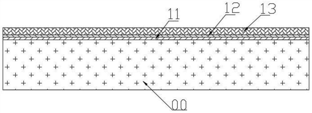
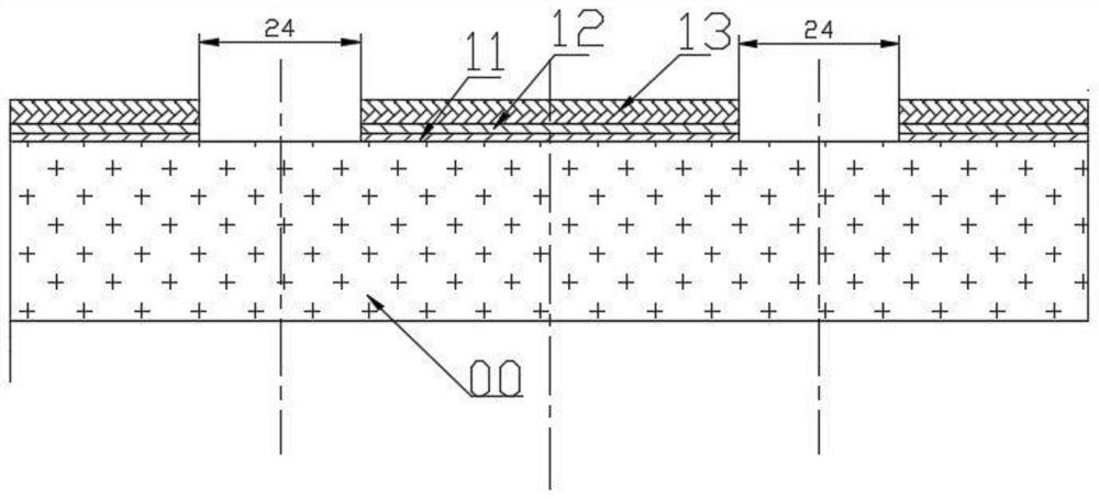
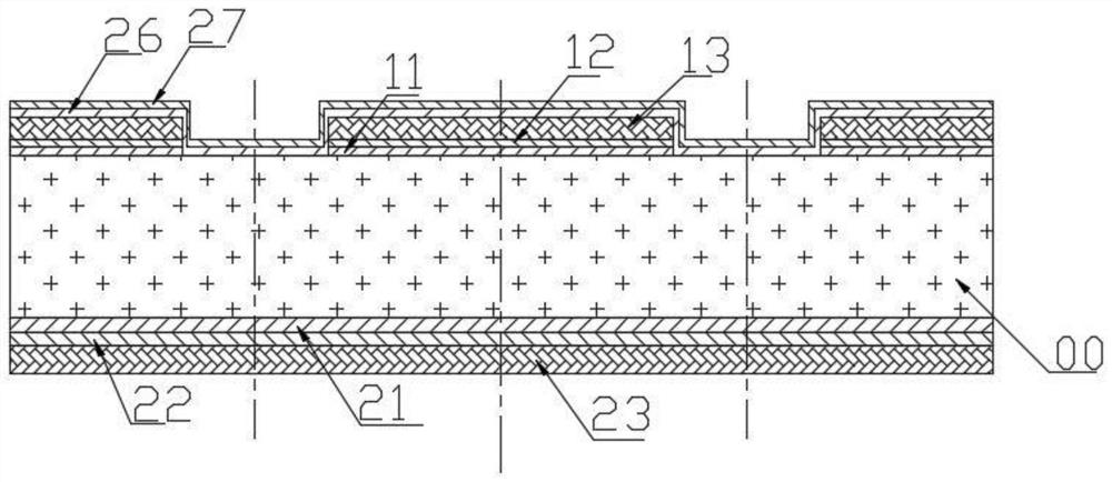
The invention provides a manufacturing method of a back contact heterojunction solar cell with low laser damage as a characteristic. The manufacturing method comprises the following steps: A, arranging a first conductive film layer of which the surface is covered with an insulating film layer on a part of a first main surface of a semiconductor substrate to form a first conductive region of a first conductive type; B, forming a second conductive film layer on the first main surface of the semiconductor substrate processed in step A; C, removing a part of the second conductive film layer covering the internal area of the first conductive area by adopting a laser non-continuous etching or laser linear etching mode; and D, removing the insulating film layer which is not covered with the second conductive film layer by adopting a chemical etching mode. The back contact heterojunction solar cell with low laser damage as the characteristic, and the manufacturing method thereof can reduce the laser damage, reduce the thermal attenuation influence and improve the photoelectric conversion efficiency.

Description

technical field [0001] The present invention relates to a back-contact heterojunction solar cell characterized by low laser damage and a manufacturing method thereof. Background technique [0002] SunPower of the United States was the first to launch mass-produced back-contact cells and modules in the world. Based on the unique advantages of back-contact technology in power generation efficiency and appearance, Panasonic’s heterojunction department has successively invested in heterojunction low-temperature back-contact technology since 2014. development, but so far, the process route of the back contact technology is relatively complicated, and frequent battery surface contact will cause damage to the surface passivation, which is not conducive to reducing the production cost of the battery and improving the mass production efficiency. 0.2% lower, and the back electrode opening technology is mainly based on ink printing and chemical etching, and the space for cost reduction...

Claims


Application Information

Patent Timeline
IPC IPC(8): H01L31/0216H01L31/0224H01L31/072H01L31/18
CPCH01L31/02168H01L31/022425H01L31/072H01L31/18Y02E10/50Y02P70/50
Inventor 谢志刚谢艺峰黄巍辉张超华林锦山林朝晖
Owner 福建金石能源有限公司
Learn More