A kind of indium phosphide bismuth nitrogen material and its preparation method, laser and detector using the material and its preparation method

A technology of indium phosphorus nitrogen bismuth and laser, which is applied in the field of materials science, can solve the problems of difficulty in doping nitrogen atoms, no way to greatly improve semiconductor performance, narrowing and other problems, and achieves suppression of Auger recombination effect, good semiconductor performance, Increase the effect of spin-orbit splitting

Active Publication Date: 2018-09-18
CHAOJING TECH BEIJING CO LTD
View PDF3 Cites 0 Cited by
  • Summary
  • Abstract
  • Description
  • Claims
  • Application Information

AI Technical Summary

Problems solved by technology

However, when nitrogen (N) atoms are doped, as the N component increases, the bond length of indium nitrogen (In-N) tends to increase, and the bond length of indium phosphorus (In-P) tends to decrease, so that In- The difference between N bond length and In-P bond length gradually increases, making the incorporation of nitrogen atoms more difficult
In this way, the band gap of indium phosphide can only be narrowed in a small range, so there is no way to greatly improve its semiconductor performance

Method used


Image

  • A kind of indium phosphide bismuth nitrogen material and its preparation method, laser and detector using the material and its preparation method
  • A kind of indium phosphide bismuth nitrogen material and its preparation method, laser and detector using the material and its preparation method
  • A kind of indium phosphide bismuth nitrogen material and its preparation method, laser and detector using the material and its preparation method

Examples


Embodiment Construction

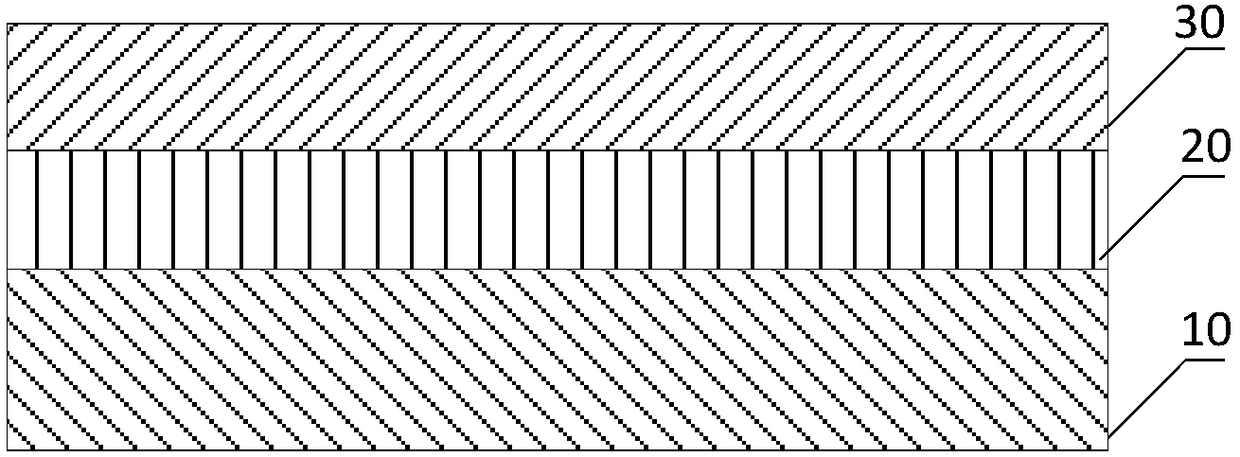
[0069] Please refer to figure 1 , in this embodiment, the indium phosphide bismuth nitrogen material includes: an indium phosphide substrate 10 , an indium phosphide buffer layer 20 and an indium phosphide bismuth nitrogen body 30 . Wherein the indium phosphide buffer layer 20 is disposed on the indium phosphide substrate. The InPBN body 30 is disposed on the InP buffer layer 20 . The chemical formula of indium phosphide bismuth nitrogen body is InP 1-x-y N x Bi y , where x and y are the concentration percentages of nitrogen atoms and bismuth atoms, respectively, and 0

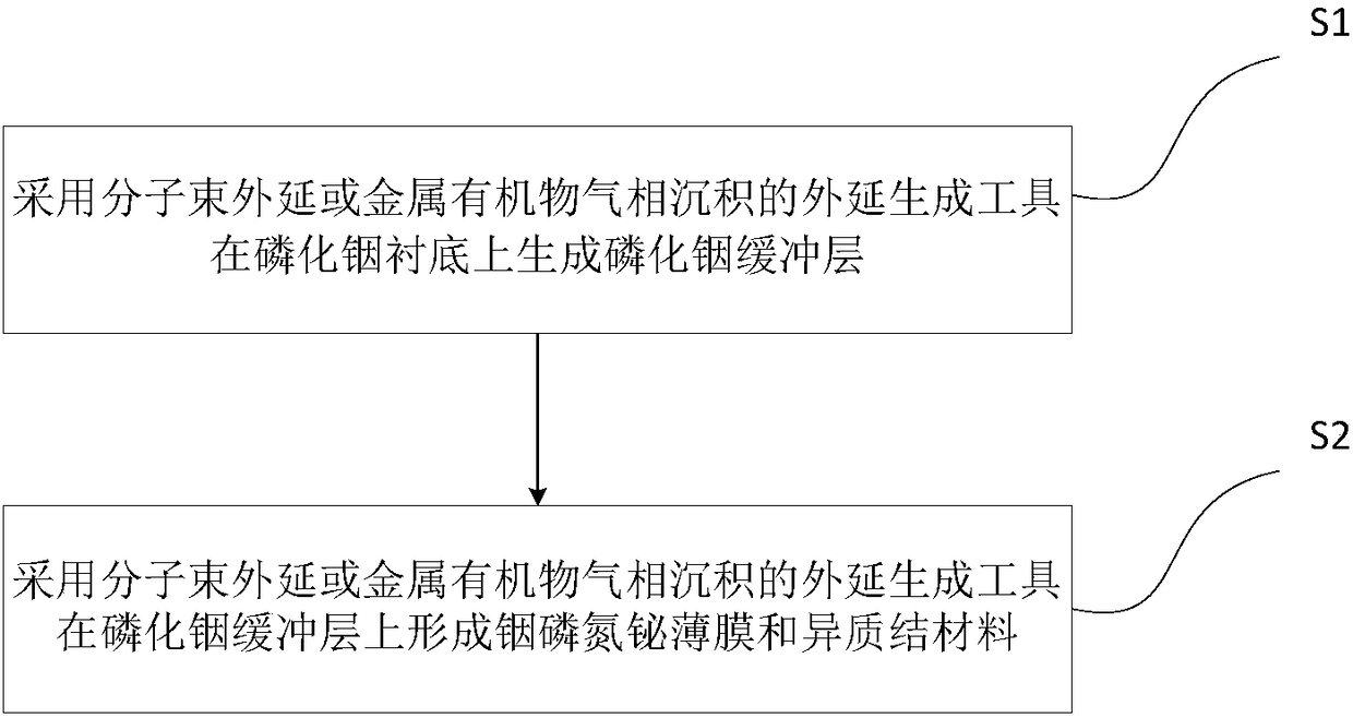
[0070] Please refer to figure 2 , in this embodiment, the preparation method of indium phosphide bismuth nitrogen material comprises the following steps:

[0071] S1: An indium phosphide buffer layer is formed on an indium phosphide substrate by molecular beam epit...


PUM

PropertyMeasurementUnit
thicknessaaaaaaaaaa
thicknessaaaaaaaaaa
thicknessaaaaaaaaaa

Abstract

The invention relates to the field of materials science, especially the indium-phosphorus-nitrogen-bismuth material, a preparation method thereof, a laser and a detector using the indium-phosphorus-nitrogen-bismuth material, and a preparation method for the laser and the detector. The indium-phosphorus-nitrogen-bismuth material comprises an indium phosphide substrate; an indium phosphide bufferinglayer which is disposed on the indium phosphide substrate; and an indium-phosphorus-nitrogen-bismuth body which is disposed on the indium phosphide buffering layer. The chemical formula of the indium-phosphorus-nitrogen-bismuth body is InP<1-x-y>N<x>Bi<y>, wherein x and y are the concentration percentages of N atoms and bismuth atoms, 0<x<11.1%, and 0<y<11.1%. The indium-phosphorus-nitrogen-bismuth material provided by the invention is smaller in energy gap width, is easier to grow and is more stable.

Description

technical field [0001] The invention relates to the field of material science, in particular to an indium phosphide bismuth nitrogen material. Background technique [0002] III-V semiconductor materials are widely used in the fields of lasers, photoelectric tubes and optical fiber communications. Among them, narrow bandgap materials have great advantages in the fields of microelectronics and optoelectronics as substrates for high-speed electronics and optoelectronic devices, and are also very suitable for vertical optical field lasers and high electron carrier transistors. Nitrogen atom is the atom with the smallest atomic radius among group V elements. Doping it into III-V group materials will affect the conduction band part of the intrinsic material and effectively control the bandgap width of the intrinsic material. That is, after nitrogen (N) atoms are individually added to indium phosphide, the band gap of indium phosphide can be further narrowed to improve its semicon...

Claims


Application Information

Patent Timeline
Patent Type & Authority Patents(China)
IPC IPC(8): H01L31/0304H01L31/109H01L31/18H01S5/343
CPCY02P70/50
Inventor 梁丹王庶民张丽
Owner CHAOJING TECH BEIJING CO LTD
Why Eureka
Try Eureka