Source-drain resistive random bidirectional switching field effect transistor and manufacturing method thereof

A field-effect transistor and bidirectional switch technology, which is applied in the direction of transistor, semiconductor/solid-state device manufacturing, electrical components, etc., can solve the problem of gate loss control, device switching performance degradation, and gate electrode's ability to control drain and source regions. and other issues, to achieve the effect of high conduction current, low sub-threshold swing, and high forward conduction current

Inactive Publication Date: 2018-03-23
山东光岳九州半导体科技有限公司
View PDF3 Cites 2 Cited by
  • Summary
  • Abstract
  • Description
  • Claims
  • Application Information

AI Technical Summary

Problems solved by technology

However, in order to realize the switching characteristics of the gate electrode of the usual Schottky barrier field effect transistor (the gate electrode is forward-conducting and reverse-blocking or reverse-conducting and forward-blocking), it is necessary to perform a specific conductivity type on the source or drain region of the device. impurity doping, which makes it difficult to achieve a good Schottky contact between the source electrode and the source region, between the drain electrode and the drain region, and the doping of the source region and the drain region makes the gate electrode to the drain The control ability of the region and the source region is reduced, resulting in a decrease in the switching performance of the device
If the semiconductor region of the device is not doped, it is easy to realize the Schottky barrier between the source electrode and the source region, and the drain electrode and the drain region in the process, but this will cause the device to have different types in the forward and reverse directions. The carrier conduction of the gate electrode, that is, both the forward bias and reverse bias of the gate electrode will make the device in the conduction state, so that the gate loses its control function as the device switching device

Method used


Image

  • Source-drain resistive random bidirectional switching field effect transistor and manufacturing method thereof
  • Source-drain resistive random bidirectional switching field effect transistor and manufacturing method thereof
  • Source-drain resistive random bidirectional switching field effect transistor and manufacturing method thereof

Examples


Embodiment Construction

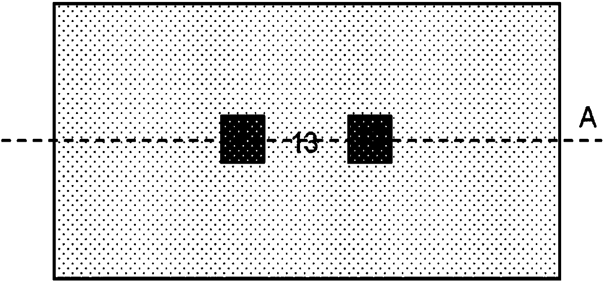
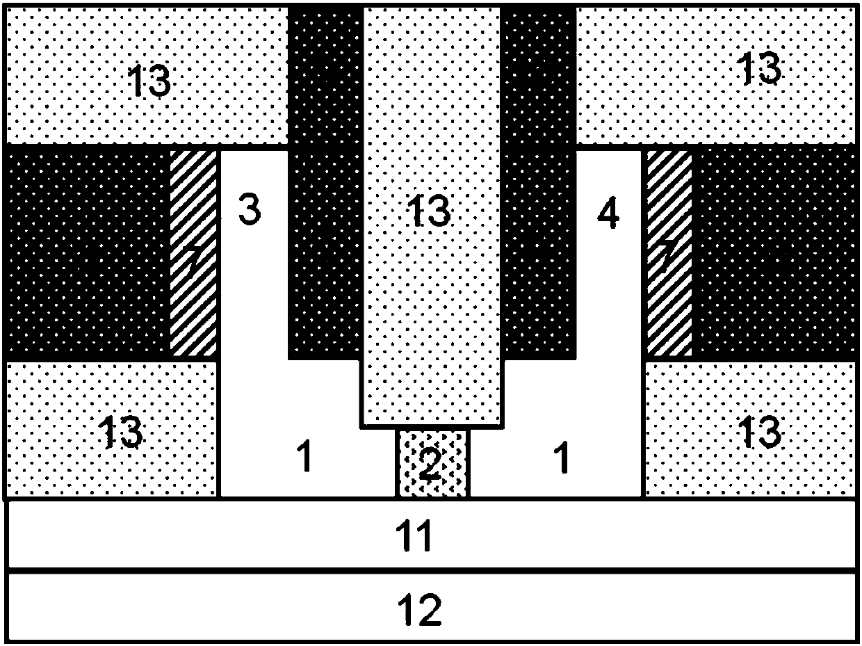
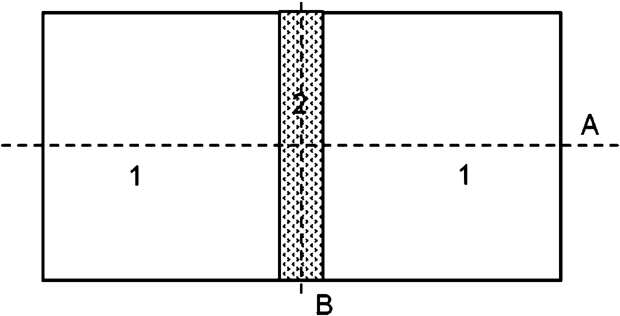
[0066] Below in conjunction with accompanying drawing, the present invention will be further described:

[0067] Such as figure 1 with figure 2 As shown, a source-drain resistance variable bidirectional switch field effect transistor comprises a silicon substrate 12 of an SOI wafer, and the silicon substrate 12 of the SOI wafer is above the substrate insulating layer 11 of the SOI wafer; Above the substrate insulating layer 11 is a part of the monocrystalline silicon film 1, the heavily doped region 2 and the insulating dielectric barrier layer 13; wherein, the monocrystalline silicon film 1 has an impurity concentration lower than 10 16 cm -3 The single crystal silicon semiconductor material; the heavily doped region 2 is located in the middle part of the bottom of the single crystal silicon film 1, and the conductivity type of the doped impurity determines the conduction type of the device, and its interior is not controlled by the field effect of the gate electrode 8, an...


PUM


Abstract

The invention relates to a source-drain resistive random bidirectional switching field effect transistor and a manufacturing method thereof. The device has the structural characteristic of bilateral symmetry, and a metal source-drain interchangeable region is controlled to act as a source region or a drain region by adjusting the source-drain interchangeable electrode voltage so as to change the direction of schottky barrier tunneling current. The device has the advantages of low static power consumption reverse leakage current and low sub-threshold swing and can realize the bidirectional switching function. Compared with the common MOSFETs type device, the intensity of the schottky barrier tunneling effect is controlled by using the gate electrode to change the resistance value of the source region and the drain region so as to realize the better switching characteristic; compared with the tunneling field effect transistor, the bidirectional switching field effect transistor has the source-drain interchangeable bidirectional symmetrical switching characteristic which is not possessed by the common tunneling field effect transistor and higher forward conduction characteristic; andcompared with the common schottky barrier transistor, the bidirectional switching field effect transistor has the advantages of high technology implementation and better reverse switching characteristic so as to be suitable for popularization and application.

Description

technical field [0001] The invention relates to the field of ultra-large-scale integrated circuit manufacturing, in particular to a source-drain resistance variable bidirectional switch field effect transistor with low leakage current suitable for low-power integrated circuit manufacturing and a manufacturing method thereof. Background technique [0002] According to the requirements of Moore's law, MOSFETs, the basic unit of integrated circuits, must become smaller and smaller in size. The resulting problem is not only the increase in the difficulty of the manufacturing process, but also the adverse effects of the device itself caused by the smaller size. highlight. Due to the limitation of the physical mechanism of current generation of MOSFETs used in integrated circuit design, the subthreshold swing cannot be lower than 60mV / dec. [0003] When ordinary tunneling field effect transistors are used as switching devices, the tunneling mechanism of carriers is used, which ca...

Claims


Application Information

Patent Timeline
Patent Type & Authority Applications(China)
IPC IPC(8): H01L29/786H01L21/336
Inventor 刘溪邹运靳晓诗
Owner 山东光岳九州半导体科技有限公司
Why Eureka
Try Eureka