Total dosage radiation-resistant FinFET device and fabrication method thereof

An anti-total dose and device technology, which is applied in semiconductor/solid-state device manufacturing, semiconductor devices, electrical components, etc., can solve the problems of device off-state leakage current increase and device off-state leakage current degradation, etc., and achieve enhanced potential control ability , reduce the off-state leakage current of the device, and weaken the effect of mutual coupling

Pending Publication Date: 2018-04-13
PEKING UNIV
View PDF4 Cites 1 Cited by
  • Summary
  • Abstract
  • Description
  • Claims
  • Application Information

AI Technical Summary

Problems solved by technology

Oxide trap charges induced by total dose radiation in shallow trench isolation (STI) regions are the main cause of device off-state leakage current increase
Especially when the Fin width is small, the degradation of the off-state leakage current of the device caused by the total dose radiation is more serious

Method used


Image

  • Total dosage radiation-resistant FinFET device and fabrication method thereof
  • Total dosage radiation-resistant FinFET device and fabrication method thereof
  • Total dosage radiation-resistant FinFET device and fabrication method thereof

Examples


Embodiment Construction

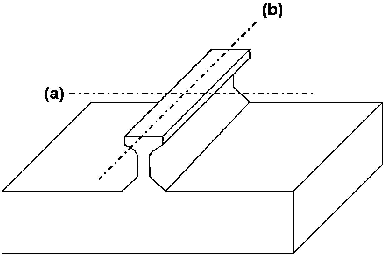
[0035] The present invention proposes a new type of FinFET device resistant to total dose radiation and its preparation method. The method forms a "dumbbell"-shaped Fin bar structure by etching, increases the distance between the STI regions on both sides of the Fin bar, and reduces device damage caused by radiation. off-state leakage current degradation. In addition, compared with ordinary bulk silicon FinFET, it has stronger gate control capability. The present invention will be described in detail below in conjunction with the accompanying drawings.

[0036] According to the following steps, a new type of bulk silicon FinFET device resistant to total dose radiation can be realized, taking NMOS as an example:

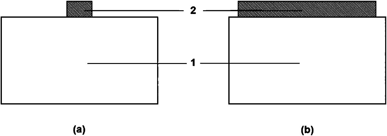
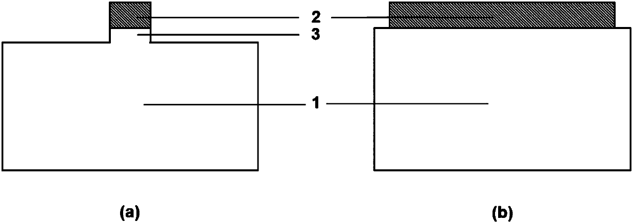
[0037] Step 1. Deposit a silicon nitride layer as a hard mask 2 on a P-type (110) silicon substrate by chemical vapor deposition (CVD), define Fin strip patterns by electron beam lithography, and etch the hard mask to expose Substrate upper surface, remove glue, suc...


PUM


Abstract

The invention discloses a total dosage radiation-resistant FinFET device and a fabrication method thereof. In the device, a dumbbell-shaped Fin strip structure is formed on a semiconductor substrate by etching, on one hand, the potential control capability of a grid on a relatively thin middle part of the dumbbell-shaped Fin strip is improved, and the influence of trap charge caused by radiation in a shallow trench isolation (STI) region on the potential of the Fin strip can be effectively reduced; and on the other hand, the distance between the STI regions at two sides of the Fin is expanded,and an off-state leakage current of the device caused by radiation is reduced. And compared with conventional body silicon FinEFT, the dumbbell-shaped Fin strip structure has the advantages that thenormal-state grid control capability of the device is also improved, and the dumbbell-shaped Fin strip structure has larger on-state current.

Description

technical field [0001] The invention relates to a Fin Field Effect Transistor (FinFET) device capable of resisting total dose radiation and a preparation method thereof, belonging to the technical field of VLSI manufacturing. Background technique [0002] In order to make the integrated circuit work normally in the harsh space radiation environment, it is necessary to put forward higher requirements on the radiation resistance performance of the device. After semiconductor devices are irradiated by electrons, X-rays, γ-rays, etc., the total dose radiation effect will occur, resulting in changes in the DC characteristics of the device, such as threshold voltage drift, increase in off-state leakage current, etc., resulting in increased power consumption and reduced performance of integrated circuits Even the function fails. With the rapid development of integrated circuit technology, the feature size of devices has been reduced to the nanometer scale. FinFET devices have goo...

Claims


Application Information

Patent Timeline
Patent Type & Authority Applications(China)
IPC IPC(8): H01L29/10H01L29/78H01L21/336
CPCH01L29/1033H01L29/66795H01L29/785
Inventor 安霞任哲玄王家宁黄如张兴
Owner PEKING UNIV
Why Eureka
Try Eureka