
Installation structure and modules

A technology for mounting structures and bumps, which is applied in the assembly of printed circuits with electrical components, semiconductor/solid-state device components, sustainable manufacturing/processing, etc., and can solve the problems of shortened signal wavelength, deterioration of connection reliability, and rising manufacturing costs.

Active Publication Date: 2020-08-07
FUJIKURA LTD
View PDF5 Cites 0 Cited by
  • Summary
  • Abstract
  • Description
  • Claims
  • Application Information

AI Technical Summary

Problems solved by technology

However, in order to multilayer the wiring board, the number of steps increases and the manufacturing cost increases.
In addition, in the structure in which the wiring is drawn downward from the terminals by multilayering, when the terminals of the semiconductor device and the terminals of the wiring board are connected by bumps, shrinkage occurs directly under the bumps due to the solidification of the solder. of stress, and thus there is a concern that the reliability of the connection deteriorates
In addition, the multilayer structure has a structure in which an interlayer insulating film is sandwiched between conductors, so there is a possibility that the transmission loss may deteriorate due to an increase in the capacitance component.
In addition, if an insulating film is placed between conductors, the wavelength of the signal transmitted to the conductors will be shortened, and the frequency characteristics will change compared to the case where the multilayer structure is not formed, so there is a problem that the design is complicated.

Method used


Image

  • Installation structure and modules
  • Installation structure and modules
  • Installation structure and modules

Examples


Embodiment 1

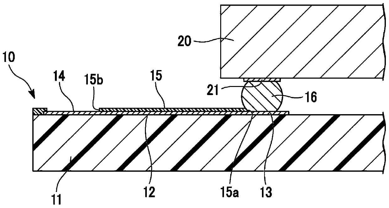
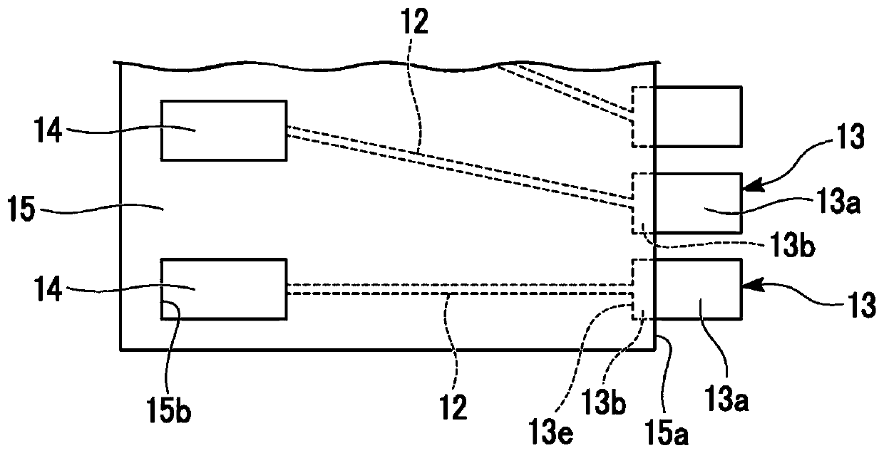
[0059] Figure 3A as well as Figure 3B The mounting structure of Example 1 is shown in . The mounting structure according to the first embodiment constitutes a module structure of an interposer substrate on which ICs are mounted as the semiconductor device 20 . The wiring board 10A of the first embodiment is an interposer substrate, and connects IC terminals (first terminals 21 ) with a narrow pitch of about 100 μm and FPC terminals (third terminals 14 ) with a wide pitch of about 500 μm.

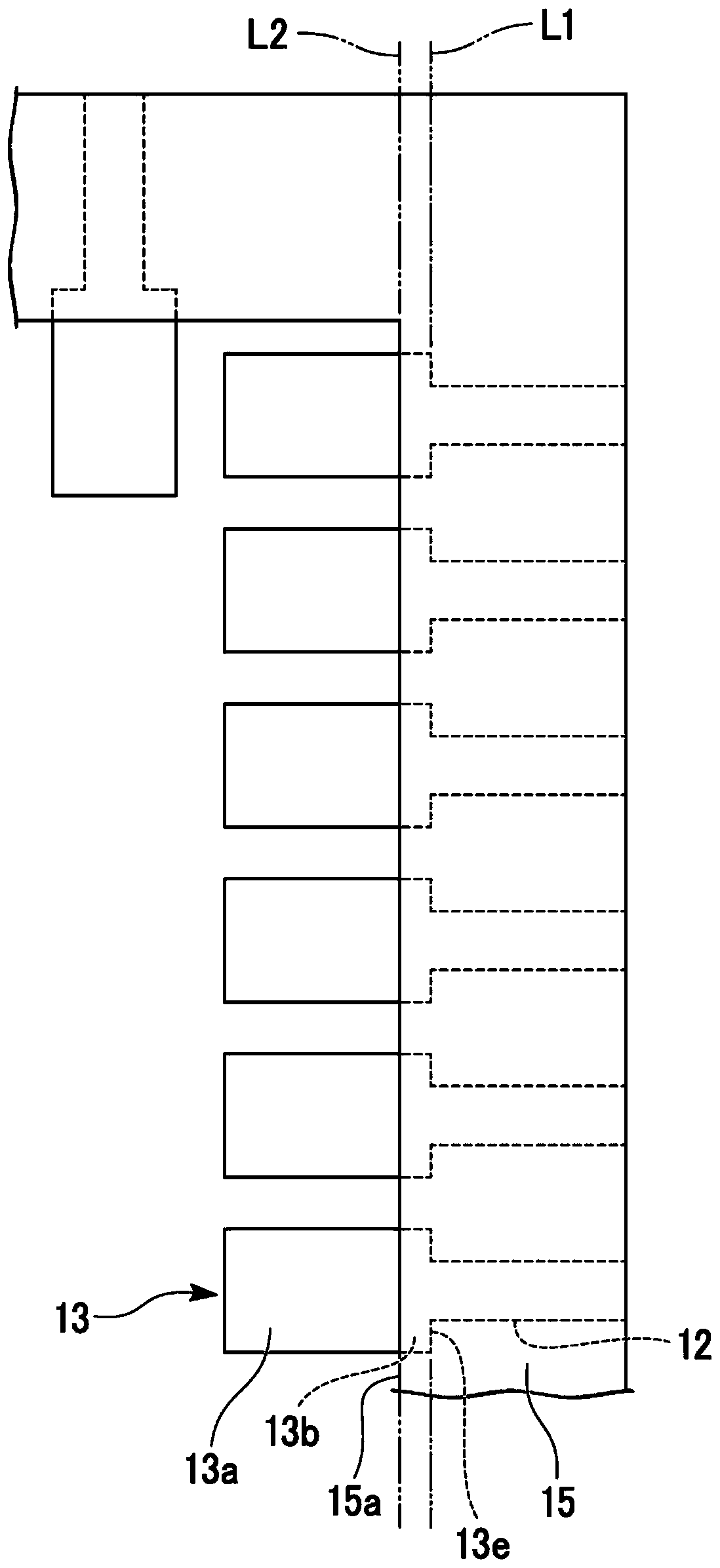
[0060] The photosensitive insulating film 15 completely covers the wiring 12 , but an opening is formed in the photosensitive insulating film 15 inside the end portion 15 a in a region surrounded by the IC I / O terminal (second terminal 13 ). The width of the second terminal 13 (the dimension in the pitch direction, the width of the second terminal 13 in the direction in which the plurality of second terminals are arranged) is, for example, 70 μm. The width of the wiring 12 is, for examp...

Embodiment 2

[0064] Figure 4A as well as Figure 4B The mounting structure of Example 2 is shown in . In the second embodiment, the structure of the wiring board 10B is the same as that of the first embodiment, but the insulating material disposed around the bump 16 is the side filler 18 . The side filler 18 (for example, epoxy-based or the like) is disposed only on the peripheral portion of the lower surface of the semiconductor device 20 where the first terminal 21 and the bump 16 are provided by adjusting the viscosity. A cavity 19 is formed between the semiconductor device 20 and the wiring board 10B (specifically, between the insulating substrate 11 ). In the case of high-frequency transmission applications, there are cases where the transmission loss deteriorates due to the dielectric between the IC and the interposer. By using the side filler 18, a gas (air, etc.) with a low dielectric constant is arranged in the cavity 19, so that the stress relaxation function can be obtained ...

Embodiment 3

[0066] Figure 5A as well as Figure 5B The mounting structure of Example 3 is shown in . The third terminal 14 of the wiring board 10C of the third embodiment constitutes a card edge connector. For the structure directly below the semiconductor device 20, in Figure 5A as well as Figure 5B Although the case of using the same underfill 17 as in Example 1 is exemplified in FIG. 1 , it is also possible to use the side filler 18 like in Example 2. The end portion 15c of the photosensitive insulating film 15 that is in contact with the card edge connector is, for example, linear.


PUM


Abstract

The present invention provides a mounting structure comprising: a semiconductor device having a first terminal; a wiring board having a second terminal, wiring, and a photosensitive insulating film, wherein the second terminal is disposed opposite to the first terminal and It has a first end portion, the wiring is led out from the end surface of the first end portion, the photosensitive insulating film covers the wiring and the first end portion; and a bump connects the first terminal and the second terminal. electrical connection between.

Description

technical field [0001] The present invention relates to a mounting structure in which a semiconductor device is mounted on a wiring board, and a module including the mounting structure. [0002] This application claims priority based on Japanese Patent Application No. 2016-038207 for which it applied to Japan on February 29, 2016, and uses the content here. Background technique [0003] In order to respond to demands for miniaturization and speedup of electronic equipment, miniaturization and speedup are also being pursued in semiconductor device mounting technologies. Flip chip bonding is adopted as a method of mounting semiconductor devices in various electronic devices due to the advantages of reducing the mounting area of ​​semiconductor devices and shortening the length of wiring compared with wire bonding. [0004] Flip-chip bonding refers to a mounting method in which a plurality of terminals of a semiconductor device such as an IC are opposed to a plurality of termi...

Claims


Application Information

Patent Timeline
Patent Type & Authority Patents(China)
IPC IPC(8): H01L21/60H05K3/34
CPCH05K3/34H01L2224/73204H01L23/49838H01L2224/0401H01L2224/16227H01L2224/32225H01L2924/15192H01L2924/351H01L2224/81447H01L2224/81439H01L2224/81424H01L2224/81455H01L2224/81444H01L2224/81471H01L2224/81466H01L2924/15323H01L2224/131H01L2224/10175H01L24/16H01L24/81H01L24/73H01L24/32H01L2924/014H01L2924/00014H01L2224/16225H01L2924/00
Inventor 松丸幸平
Owner FUJIKURA LTD
Learn More