Infrared light perfect absorber and preparation method thereof

An infrared light and absorber technology, applied in optics, instruments, filters, etc., can solve the problem of large area, low-cost preparation, inability to effectively expand electronic control or optoelectronic functional device platforms, and inability to achieve infrared broadband or infrared ultra-high Broadband light absorption and other issues, to achieve the effect of reducing cost requirements, easy large-area preparation, and simple structure

Inactive Publication Date: 2018-04-20
JIANGXI NORMAL UNIV
View PDF2 Cites 12 Cited by
  • Summary
  • Abstract
  • Description
  • Claims
  • Application Information

AI Technical Summary

Problems solved by technology

Therefore, this kind of three-layer structured optical perfect absorber is difficult to manufacture in a large area and at low cost, and thus cannot be effectively expanded to electronically controlled or optoelectronic functional device platforms.
In addition, these three-layer structured light perfect absorbers often can only absorb electromagnetic waves of a single resonance wavelength, which is narrow-band light absorption, that is, they cannot achieve infrared broadband or infrared ultra-broadband light absorption.

Method used


Image

  • Infrared light perfect absorber and preparation method thereof
  • Infrared light perfect absorber and preparation method thereof
  • Infrared light perfect absorber and preparation method thereof

Examples


Embodiment 1

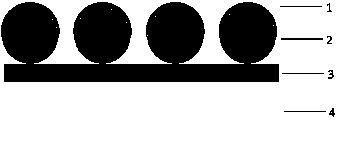
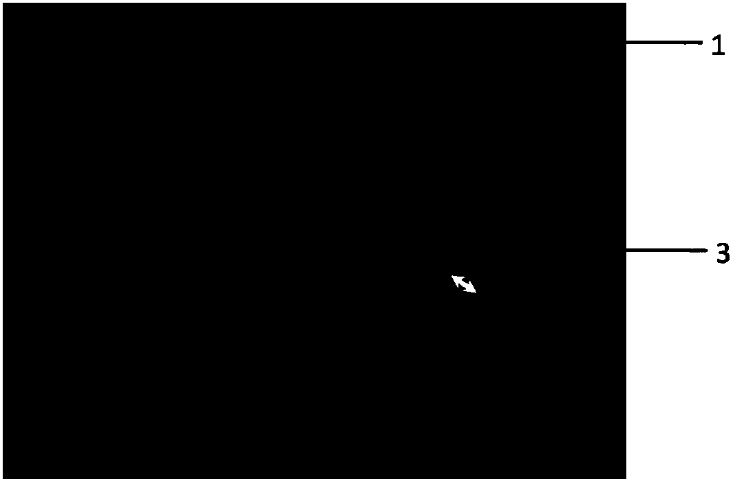
[0034] figure 1 It is a schematic side view of an infrared light perfect absorber structure according to an embodiment of the present invention, figure 2 It is a schematic top view of the structure of an infrared light perfect absorber according to the embodiment of the present invention. Such as figure 1 and figure 2 As shown, the infrared light perfect absorber provided by the present invention includes a substrate 4, an opaque metal film layer 3 arranged on the substrate 4, and a colloidal crystal-metal thin film resonant film layer arranged on the metal film layer 3 structural layer. Wherein, the colloidal crystal-metal film resonance structure layer is composed of a plurality of identical colloidal crystal particles 2 and a metal film 1 deposited on the upper surface of each colloidal crystal particle 2 . The colloidal crystal particles 2 are evenly arranged on the metal film layer 3 , that is, the colloidal crystal-metal film resonance structure is a non-close-pack...

Embodiment 2

[0053] The substrate 4 of the infrared light perfect absorber provided by Embodiment 2 of the present invention is a silicon wafer, the metal material is gold, the thickness of the metal film layer 3 is 100 nm, the material of the colloidal crystal particles 2 is polystyrene, and the colloidal crystal particles 2 are engraved The diameters before and after etching are 1000 nm and 700 nm respectively, that is, the gap g between adjacent colloidal crystal particles 2 after etching is 300 nm. The metal thin film 1 in the colloidal crystal-metal thin film resonance structure layer is a gold film, and the thickness of the metal thin film 1 is 15nm.

[0054] Figure 4 It is the light absorption figure of the infrared light perfect absorber provided by the second embodiment of the present invention, such as Figure 4 As shown, it can be found from the spectrogram of the experimental test that the maximum absorption rate reaches 98% in the 1.541 micron band, and the absorption rate i...

Embodiment 3

[0056] The substrate 4 of the infrared light perfect absorber provided by Embodiment 3 of the present invention is glass, the metal material is gold, the thickness of the metal film layer 3 is 100nm, the material of the colloidal crystal particles 2 is polystyrene, and the colloidal crystal particles 2 are etched The front and rear diameters are 1000 nm and 600 nm respectively, that is, the gap g between adjacent colloidal crystal particles 2 after etching is 400 nm. The metal thin film 1 in the colloidal crystal-metal thin film resonance structure layer is a gold film, and the thickness of the metal thin film 1 is 15nm.

[0057] Figure 5 It is the light absorption figure of the infrared light perfect absorber provided by Embodiment 3 of the present invention, as Figure 5 As shown, it can be found from the spectrogram that the maximum absorption rate reaches 99% in the 1.258 micron band, and 99.9% in the 1.266 micron band. In addition, the absorbance in the spectral range ...


PUM


Abstract

The invention discloses an infrared light perfect absorber and a preparation method thereof, and aims at introducing a colloidal crystal material, utilizing electromagnetic resonance characteristics of a plasmonic element and a colloidal crystal on a metal surface, and adopting a colloid self-assembling method to prepare an infrared light perfect absorber that includes a substrate, a light-proof metal film layer on the substrate and a colloidal crystal-metal thin film resonance structure layer disposed on the metal film layer. The colloidal crystal-metal thin film resonance structure layer iscomposed of multiple identical colloidal crystal particles and a metal thin film deposited on the upper surface of each of the colloidal crystal particles. The colloidal crystal particles are uniformly arranged on the metal film layer. With the colloidal crystal-metal thin film resonance structure layer, the structure of an absorption unit of an original infrared light perfect absorber is simplified, the bandwidth of the absorption spectrum of the infrared light perfect absorber is increased, and the preparation requirements of low cost and easy large-area preparation are satisfied by using the colloid self-assembling method.

Description

technical field [0001] The invention relates to the fields of photoelectric functional materials and devices and photonics, in particular to an infrared light perfect absorber and a preparation method thereof. Background technique [0002] The optical perfect absorber is an essential component to realize high-efficiency spectral light absorption and photodetection, and it can realize the absorption of light wave energy in a specific band or multiple band spectral ranges. The principle of the optical perfect absorber is generally that the optical resonance mode of the dielectric guided wave, the metal plasmon resonance, and the spectral phase coupling or coherence cause the resonant absorption or trapping of the light wave. Optically perfect absorbers in the near-infrared and mid-infrared bands can be used as building blocks for photoelectric converters, thermal emitters, or as coating materials to reduce stray emissions of electromagnetic waves. [0003] The research on ele...

Claims


Application Information

Patent Timeline
Patent Type & Authority Applications(China)
IPC IPC(8): G02B5/22G02B5/20G02B5/00G02B1/00
CPCG02B1/00G02B5/008G02B5/208G02B5/22
Inventor 刘正奇刘桂强黄镇平张后交陈戬余美东
Owner JIANGXI NORMAL UNIV
Why Eureka
Try Eureka