A fan-out wafer level chip packaging structure and packaging method

A wafer-level chip and packaging structure technology, which is applied in semiconductor/solid-state device parts, semiconductor devices, electrical components, etc., can solve the problems of high production cost and difficult preparation of fan-out wafer-level chip packaging structure, etc. Achieve the effect of less difficulty in preparation, improve heat dissipation performance, and improve manufacturing precision

Active Publication Date: 2020-03-10
NAT CENT FOR ADVANCED PACKAGING CO LTD
View PDF7 Cites 0 Cited by
  • Summary
  • Abstract
  • Description
  • Claims
  • Application Information

AI Technical Summary

Problems solved by technology

[0005] Therefore, the technical problem to be solved by the present invention is to solve the problem that the preparation of the electromagnetic shielding structure in the fan-out wafer-level chip packaging structure is relatively difficult, and the production cost of the fan-out wafer-level chip packaging structure is relatively high.

Method used


Image

  • A fan-out wafer level chip packaging structure and packaging method
  • A fan-out wafer level chip packaging structure and packaging method
  • A fan-out wafer level chip packaging structure and packaging method

Examples


Embodiment 1

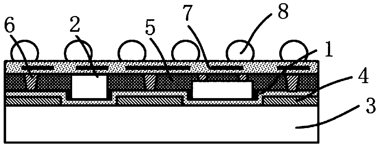
[0032] This embodiment provides a fan-out wafer level chip packaging structure, such as figure 1 As shown, it includes: conductive layer 1, a groove for setting chip 2 is formed on conductive layer 1; conductive layer 1 is arranged on substrate 3; insulating layer 4 is arranged between conductive layer 1 and substrate 3 for filling The gap between the conductive layer 1 and the substrate 3; the package 5 is arranged on the upper surface of the conductive layer 1; the chip 2 is packaged in the package 5, and the pad of the chip 2 is exposed outside the package 5; the conductive column 6 is set In the package body 5 , one end is coupled to the conductive layer 1 , and the other end is exposed outside the package body 5 ; the conductive post 6 is connected to the ground wire. In a specific embodiment, the depth of the groove is smaller than the thickness of the chip 2, and the conductive layer 1 is aluminum, copper, aluminum alloy or copper alloy layer. Preferably, the thickness ...

Embodiment 2

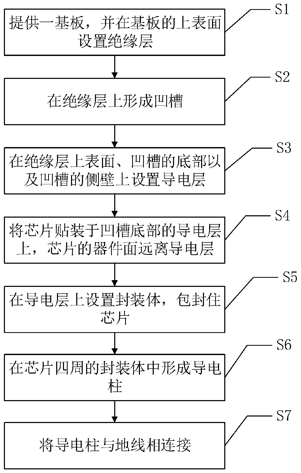
[0040] This embodiment provides a fan-out wafer level chip packaging method, such as figure 2 As shown, including the following steps:

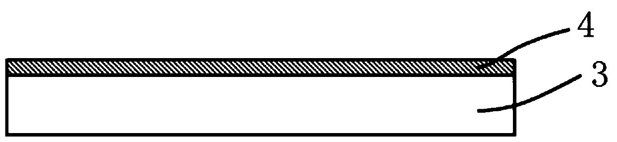
[0041] Step S1: providing a substrate, and disposing an insulating layer on the upper surface of the substrate. Such as image 3 As shown, in this embodiment, the insulating layer 4 may be provided by spray coating or spin coating. In a specific embodiment, the material of the substrate 3 is a material with good thermal conductivity such as silicon, silicon carbide, thermally conductive ceramics or metal, and the insulating layer 4 is a photosensitive material layer prepared by photosensitive polyimide or other photosensitive resins. Of course, it can also be a non-photosensitive material layer. Preferably, the thickness of the insulating layer 4 is 2-20um.

[0042] Step S2: forming grooves on the insulating layer. Such as Figure 4 As mentioned above, in a specific embodiment, when the insulating layer 4 is a photosensitive material la...


PUM


Abstract

The present invention provides a fan-out wafer-level chip packaging structure and a packaging method, wherein the fan-out wafer-level chip packaging structure includes: a conductive layer, on which grooves for setting chips are formed; On the substrate; the insulating layer is arranged between the conductive layer and the substrate, and is used to fill the gap between the conductive layer and the substrate; the package is arranged on the upper surface of the conductive layer; the chip is packaged in the package, and the pad of the chip exposed outside the package; the conductive post is arranged in the package, one end is coupled with the conductive layer, and the other end is exposed outside the package; the conductive post is connected to the ground wire. By placing the chip in the groove on the conductive layer, and the conductive layer is connected to the ground wire through the conductive column, an electromagnetic shielding structure inside the fan-out wafer-level chip packaging structure can be formed, which can reduce the impact of the chip on the packaging structure. The possibility of electromagnetic wave interference of internal devices and external devices is less difficult to prepare and the production cost is lower.

Description

technical field [0001] The invention relates to the technical field of semiconductor packaging, in particular to a fan-out wafer-level chip packaging structure and packaging method with an electromagnetic shielding structure. Background technique [0002] With the popularity of wireless electronic devices, the integration of radio frequency chips is getting higher and higher, and fan-out packaging technology is increasingly used in radio frequency chip packaging. As the number of radio-frequency devices in the package increases, the direct electromagnetic interference between devices and modules, modules and modules becomes more and more prominent. It is more and more important to implement electromagnetic shielding structures in the fan-out packaging process. The conventional method is to apply an electromagnetic shielding metal shell outside the package body after the package is completed, but the metal shell increases the cost of the package and increases the volume of th...

Claims


Application Information

Patent Timeline
Patent Type & Authority Patents(China)
IPC IPC(8): H01L23/13H01L23/367H01L23/544H01L23/552H01L21/48
CPCH01L21/4871H01L23/13H01L23/3672H01L23/544H01L23/552H01L2224/12105H01L2224/73267H01L2924/15153
Inventor 姚大平
Owner NAT CENT FOR ADVANCED PACKAGING CO LTD
Why Eureka
Try Eureka