Trench-gate superjunction device and manufacturing method thereof

A technology of super junction devices and manufacturing methods, which is applied in the field of trench gate super junction devices and trench gate super junction devices, and can solve the problems of application system current and voltage overshoot, circuit failure, circuit damage, etc.

Active Publication Date: 2018-05-04
SHENZHEN SANRISE TECH CO LTD
View PDF3 Cites 4 Cited by
  • Summary
  • Abstract
  • Description
  • Claims
  • Application Information

AI Technical Summary

Problems solved by technology

The existence of these two factors makes the switching process of the super junction MOSFET prone to excessively low Crss and sharp changes in Crss, resulting in too fast a switching process, resulting in large electromagnetic interference in the application system of the device; even due to the current and voltage Overshoot and cause the circuit to fail
[0019] like image 3 In the structure shown, in the process of the device changing from the on-state to the reverse-off state, in the plateau voltage stage, the Vgs of the device, that is, the gate-source voltage, remains at the plateau voltage, and the Vds, that is, the drain-source voltage of the device, is kept at the plateau voltage when the device is turned on. The Vdson (usually very small) is increased to the power supply voltage Vdd (such as 400 volts) of the circuit. Due to the increase of Vds, the adjacent P-type column 4 and N-type column 3 are laterally depleted, and the N-type column is depleted at a certain voltage. Part or all of the type column 3 is completely depleted, and now the Cgd of the device will become very small, Cgd is Crss, and Cgd is the series connection of Cox and Csi, because dVds / dt=Igp / Cgd (Vds), wherein Vds is the drain The source voltage, the gate current when Igp is the platform voltage, dVds / dt will become very large at this voltage; in this process, the di / dt caused by the nonlinearity of the capacitance is too large, which will also cause the system or device The voltage on the parasitic inductance will overshoot (Ldi / dt), where i is the source leakage current, and L is the parasitic inductance. These factors will cause electromagnetic interference in the circuit or system using the device, affecting the normal operation of the circuit and system ; This situation also exists during the change from the high-voltage reverse cut-off state to the conduction state
This high dVds / dt during the switching process, in addition to causing the oscillation of the application circuit, may also cause excessive current and voltage overshoot of the application system, resulting in circuit damage

Method used


Image

  • Trench-gate superjunction device and manufacturing method thereof
  • Trench-gate superjunction device and manufacturing method thereof
  • Trench-gate superjunction device and manufacturing method thereof

Examples


Embodiment 1

[0116] Embodiment of the present invention a trench gate super junction device:

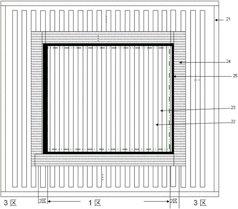
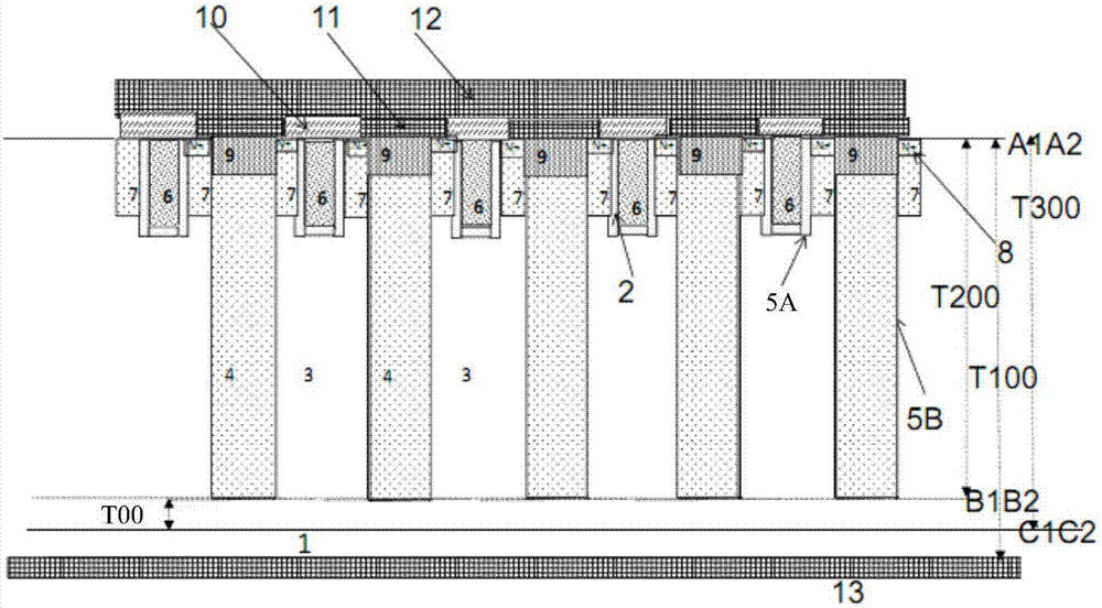
[0117] Such as Figure 4 Shown is a schematic top view of a superjunction device according to an embodiment of the present invention; Figure 5A is along Figure 4 Schematic cross-sectional view of the centerline C2; Figure 5B is along Figure 4 Schematic cross-sectional view of the center line C3; Figure 5C is along Figure 4 Schematic cross-sectional view of the center line C4; Figure 5D is along Figure 4 Schematic cross-sectional view of the center line C1;

[0118] Embodiment 1 of the present invention, a superjunction device includes a charge flow region, a termination region laterally subjected to a reverse bias voltage, and a transition region between the charge flow region and the termination region, and the termination region surrounds the periphery of the charge flow region, including For the structure of the entire charge flow region, transition region and terminal region, pl...

Embodiment 2

[0144] Embodiment 2 of the present invention Trench gate super junction device:

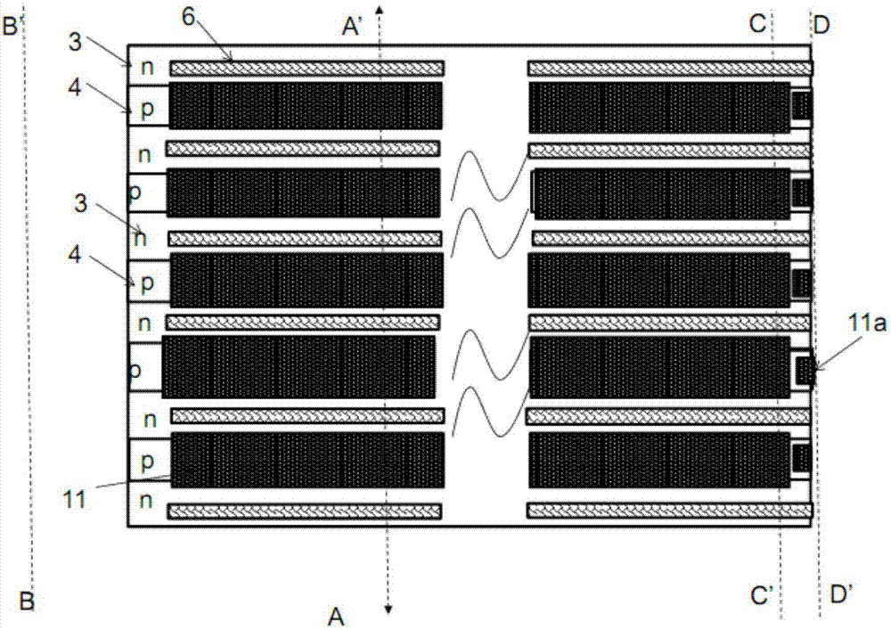
[0145] Such as Image 6 As shown, it is a schematic top view of a trench gate super junction device in Embodiment 2 of the present invention; the difference between the trench gate super junction device in Embodiment 2 of the present invention and the trench gate super junction device in Embodiment 1 of the present invention is that the present invention Embodiment 2 In the trench-gate superjunction device: a contact region 9 composed of a P+ region is formed on the top of each floating P-type column 4a extending into the transition region, and a contact region 9 is formed on the top of the contact region 9 and connected to The contact hole 11b to said source, ie the contact hole marked with the reference 11b alone. After the contact hole 11b is formed, the two ends of the floating P-type column 4a will be connected to the source, but the middle area located in the charge flow region will not be...

Embodiment 3

[0146] Three-trench gate super-junction device according to the embodiment of the present invention:

[0147] Such as Figure 7 As shown, it is a schematic top view of the three-trench gate super-junction device of the embodiment of the present invention; the difference between the three-trench gate super-junction device of the embodiment of the present invention and the first trench gate super-junction device of the present invention is that the present invention In the trench gate super junction device of the third embodiment: a P-type ring 7a is formed on the surface of the super junction structure in the transition region, and a contact region 9 composed of a P+ region is formed on the top of the P-type ring 7a and formed A contact hole 11c on top of the contact region 9 and connected to the source. The doping concentration of the P-type ring 7a is the same as that of the P-type well 7; or, the doping concentration of the P-type ring 7a is different from that of the P-typ...


PUM

PropertyMeasurementUnit
Thicknessaaaaaaaaaa
Thicknessaaaaaaaaaa
Thicknessaaaaaaaaaa

Abstract

The invention discloses a trench-gate superjunction device. A P-type post is divided to an electrode connection P-type post and a floating P-type post which form a first periodic arrangement structurewith a step larger than that of a superjunction unit, a P-type well and a contact hole are formed in the top of the electrode P-type post, the P-type well extends to an N-type post, the contact holeis connected with a source, the P-type well and the contact hole are not formed in the top of the floating P-type post, a length direction of a trench gate and a length direction of the superjunctionstructure are perpendicular to each other and are arranged to form a second periodic arrangement structure, and the step of the second periodic arrangement structure is independently adjusted. The invention also discloses a manufacturing method of the trench-gate superjunction device. By the trench-gate superjunction device, the breakdown voltage and the channel density of the device can be improved, the conduction resistance is reduced, higher Crss can be obtained under very low Vds, the Crss can be slowly reduced within a relatively large Vds range, the speed of the switch process can be reduced, the electromagnetic interference performance of the device in an application circuit can be effectively reduced, and overshoot of a current and a voltage brought by the device in the applicationcircuit can be effectively reduced.

Description

technical field [0001] The invention relates to the field of semiconductor integrated circuit manufacturing, in particular to a trench gate superjunction (superjunction) device; the invention also relates to a manufacturing method of the trench gate superjunction device. Background technique [0002] The super junction structure is composed of alternately arranged N-type pillars and P-type pillars. If the superjunction structure is used to replace the N-type drift region in the vertical double-diffused MOS transistor (Vertical Double-diffused Metal-Oxide-Semiconductor, VDMOS) device, the conduction path is provided through the N-type column in the conduction state, and when the conduction The P-type column does not provide a conduction path; in the off state, the PN column jointly bears the reverse bias voltage, forming a super-junction metal-oxide-semiconductor field-effect transistor (Metal-Oxide-Semiconductor Field-Effect Transistor, MOSFET). The super-junction MOSFET ca...

Claims


Application Information

Patent Timeline
IPC IPC(8): H01L29/78H01L29/06H01L21/336
CPCH01L29/0634H01L29/66734H01L29/7813
Inventor 肖胜安曾大杰李东升
Owner SHENZHEN SANRISE TECH CO LTD
Why Eureka
Try Eureka