LED packaging method

A technology of LED packaging and heat dissipation substrate, applied in semiconductor devices, electrical components, circuits, etc., can solve the problems of affecting the heat dissipation effect, insufficient contact of the bottom surface of the heat sink, affecting the light transmission efficiency, etc. Heat dissipation effect, effect of reducing manufacturing cost

Active Publication Date: 2018-05-08
廊坊源驰科技有限公司
View PDF3 Cites 0 Cited by
  • Summary
  • Abstract
  • Description
  • Claims
  • Application Information

AI Technical Summary

Problems solved by technology

Finally, because high-power LEDs are used in lighting and other occasions, cost control is very important, and the structural size of the external heat sink of high-power LED lamps is not allowed to be too large, and it is impossible to allow active cooling by adding electric fans and other methods. The safe junction temperature should be within 110°C. If the junction temperature is too high, it will lead to a series of problems such as reduced light intensity, spectral shift, increased color temperature, increased thermal stress

Method used


Image

  • LED packaging method
  • LED packaging method
  • LED packaging method

Examples


Example Embodiment

[0055] Embodiment one

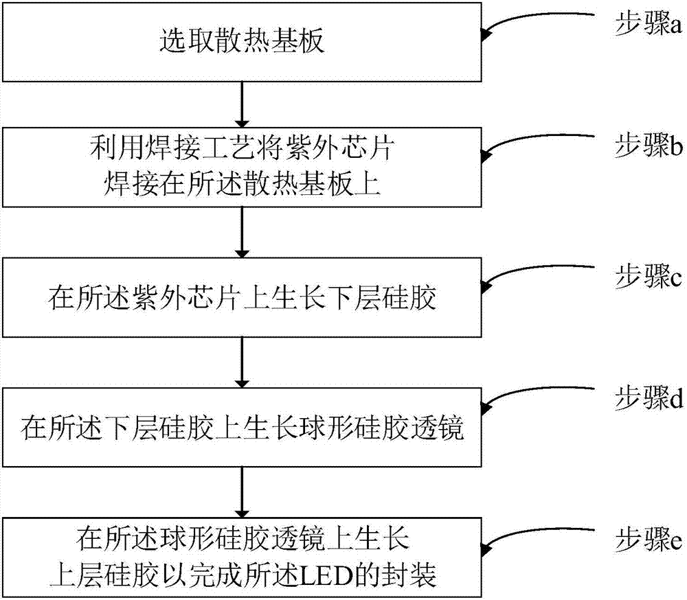
[0056] See figure 1 , figure 1 It is a flow chart of an LED packaging method provided by an embodiment of the present invention. The method comprises the steps of:

[0057] Step a, selecting a heat dissipation substrate;

[0058] Step b, using a welding process to weld the ultraviolet chip on the heat dissipation substrate;

[0059] Step c, growing the lower layer of silica gel on the ultraviolet chip;

[0060] Step d, growing spherical silica gel lenses on the lower layer of silica gel;

[0061] Step e, growing an upper layer of silica gel on the spherical silica gel lens to complete the packaging of the LED.

[0062] Preferably, the heat dissipation substrate is made of iron and has a thickness of 0.5-10mm.

[0063] Preferably, circular through-holes along the width direction and parallel to the plane of the heat-dissipating substrate are provided inside the heat-dissipating substrate; wherein, the diameter of the circular through-holes is 0.2-0....

Example Embodiment

[0093] Embodiment two

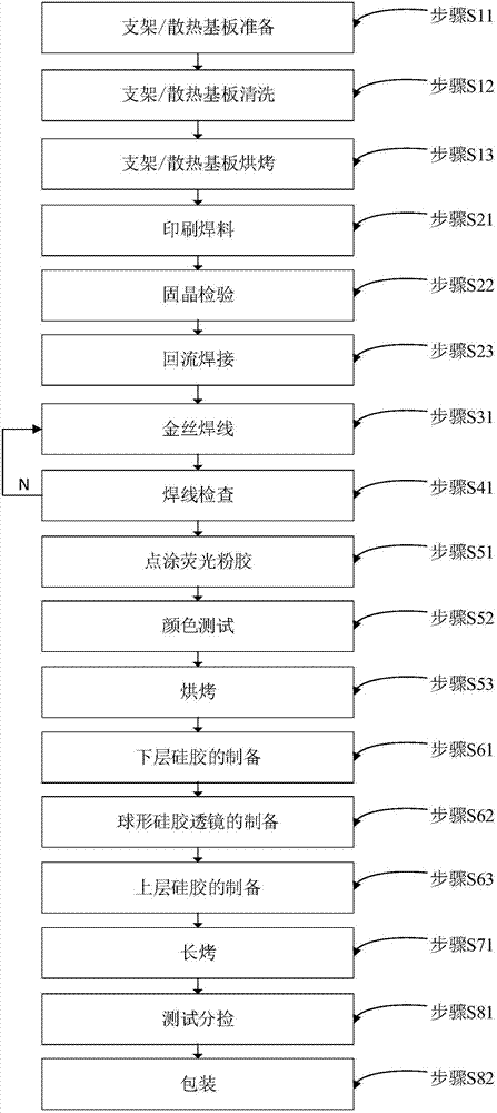
[0094] See figure 2 , figure 2 It is a schematic flow chart of an LED packaging method provided by an embodiment of the present invention. On the basis of the above embodiments, this embodiment will introduce the process flow of the present invention in more detail. The method includes:

[0095] S1, preparation of heat dissipation substrate;

[0096] S11, preparation of support / radiation substrate;

[0097] Specifically, select a heat dissipation substrate 101 with a thickness of 0.5-10 mm and a material of iron, and cut the heat dissipation substrate 101;

[0098] S12. Cleaning of the support / heat dissipation substrate;

[0099] Specifically, clean the stains on the heat dissipation substrate 101 and the support, especially the oil stains;

[0100] S13, baking of the bracket / radiation substrate;

[0101] Specifically, the cleaned heat dissipation substrate 101 and the support are baked to keep the heat dissipation substrate 101 and the suppor...

Example Embodiment

[0140] Embodiment Three

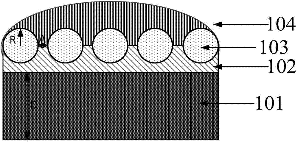
[0141] Please also see image 3 , Figure 4 , Figure 5 , Image 6 , Figure 7a ~ Figure 7b , image 3 A schematic cross-sectional view of an LED package structure provided by an embodiment of the present invention, Figure 4 A cross-sectional schematic diagram of another LED package structure provided by an embodiment of the present invention, Figure 5 A schematic cross-sectional view of a heat dissipation substrate provided by an embodiment of the present invention, Image 6 A schematic cross-sectional view of an ultraviolet wick provided by an embodiment of the present invention, Figure 7a A schematic cross-sectional view of a spherical silicone lens provided by an embodiment of the present invention, Figure 7b A schematic cross-sectional view of another spherical silicone lens provided by an embodiment of the present invention. The LED packaging structure includes:

[0142] heat dissipation substrate 101;

[0143] Among them, such as...


PUM

PropertyMeasurementUnit
Thicknessaaaaaaaaaa
Wavelengthaaaaaaaaaa

Abstract

The invention relates to an LED packaging method, which comprises the steps of selecting a heat dissipation substrate; welding an ultraviolet chip on the heat dissipation substrate by using a weldingprocess; growing lower silica gel on the ultraviolet chip; growing a spherical silica gel lens on the lower silica gel; and growing upper silica gel on the spherical silica gel lens to complete packaging of an LED. According to an LED packaging structure, the heat dissipation effect of the LED is improved by adopting the iron heat dissipation substrate with a through hole structure; the conditionthat an LED chip can better irradiate outwards through a packaging material can be ensured by adopting a spherical silica gel lens structure; and the light transmittance is improved.

Description

technical field [0001] The invention relates to the technical field of LED packaging, in particular to an LED packaging method. Background technique [0002] As a new type of solid-state light source, LED has many advantages such as small size, high luminous efficiency, low energy consumption, long life, no mercury pollution, all solid state, quick response, low working voltage, safety and reliability, etc. And other fields have very broad application prospects and market economic benefits, and are expected to become a new generation of green and environmentally friendly lighting sources to replace the existing fluorescent lamps and incandescent lamps, so they have received extensive attention from researchers at home and abroad. [0003] In recent years, LEDs mostly use blue wicks plus yellow fluorescent light to generate white light to achieve lighting. This method has the following problems. [0004] First of all, the light emitted by the LED light source is generally di...

Claims


Application Information

Patent Timeline
IPC IPC(8): H01L33/50H01L33/56H01L33/58H01L33/64
CPCH01L33/504H01L33/507H01L33/56H01L33/58H01L33/641H01L33/648H01L2933/005H01L2933/0058
Inventor 张亮
Owner 廊坊源驰科技有限公司
Why Eureka
Try Eureka