Method of preparing high heat dissipating ceramic package substrate

A ceramic packaging and ceramic substrate technology, which is applied in semiconductor/solid-state device manufacturing, electrical components, electric solid-state devices, etc., can solve the problems of poor bonding between conductive lines and ceramic substrates, high production costs, and complicated process routes. To achieve the effect of ensuring product yield, avoiding ceramic cracking and conductive line falling off, and simplifying the process flow

Active Publication Date: 2018-05-18
DONGGUAN INST OF OPTO ELECTRONICS PEKING UNIV
View PDF8 Cites 6 Cited by
  • Summary
  • Abstract
  • Description
  • Claims
  • Application Information

AI Technical Summary

Problems solved by technology

However, because the formed aluminum layer is very thin and not dense enough, there will be a problem of poor bonding between the conductive circuit and the ceramic substrate; Chinese patent CN102452843B forms copper oxide on the surface of the copper plate in advance, and then forms an aluminum oxide layer with the pre-oxidized surface Aluminum nitride ceramic substrates are stacked and sintered in an inert atmosphere to reduce copper oxide to cuprous oxide to form the precursor of ceramic copper-clad laminates, and then sinter again to form circuits
However, this method has the problem of controlling multiple sinterings, and at the same time, a subsequent etching process is required to obtain conductive lines, and the complexity of the process route will lead to high production costs.

Method used


Image

  • Method of preparing high heat dissipating ceramic package substrate
  • Method of preparing high heat dissipating ceramic package substrate
  • Method of preparing high heat dissipating ceramic package substrate

Examples


Embodiment 1

[0034] A method for preparing a high heat dissipation ceramic packaging substrate, comprising the following steps:

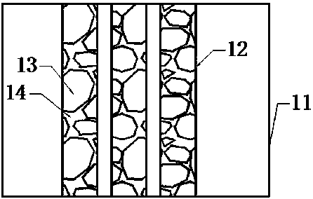
[0035] S1, as attached figure 1 As shown, the cleaned aluminum nitride ceramic substrate 11 is placed on the platform of a marking machine with a laser of 355nm, and according to the set circuit pattern, the 5J / cm 2 The laser energy density was used to mark the ceramic substrate 10 times in the air atmosphere, so that a mixture layer with a metallized circuit pattern 12 was formed on the marking line. The thickness of the mixture layer was 4 μm, and the mixture layer was composed of alumina 13 and aluminum 14. Areas of the ceramic substrate that are not laser marked remain insulated.

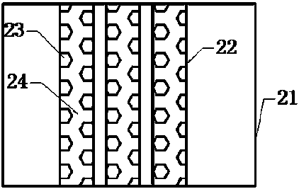
[0036] S2, as attached figure 2 As shown, the aluminum nitride ceramic substrate 21 that has been marked and formed a mixture layer of a metallized circuit pattern is immersed in an electroless copper plating solution at 55° C. for electroless copper plating. The soaking time i...

Embodiment 2

[0041] S1, as attached figure 1 As shown, the cleaned aluminum nitride ceramic substrate 11 is placed on the platform of a marking machine with a laser of 355nm, and according to the set circuit pattern, the 20J / cm 2engrave the ceramic substrate 5 times in the air atmosphere, so that a mixture layer of metallized circuit pattern 12 is formed on the marked circuit, the thickness of the mixture layer is 3 μm, and the mixture layer is composed of alumina 13 and aluminum 14. Areas of the ceramic substrate that are not laser marked remain insulated.

[0042] S2, as attached figure 2 As shown, the aluminum nitride ceramic substrate that has been marked and formed a mixture layer of a metallized circuit pattern is immersed in an electroless copper plating solution at 60°C for electroless copper plating. The immersion time is 25 minutes, so that the marked circuit area forms about A 6 μm thick bonding layer composed of oxide and elemental metal, the oxide is cuprous oxide 23 , and ...


PUM

PropertyMeasurementUnit
thicknessaaaaaaaaaa
thicknessaaaaaaaaaa
thicknessaaaaaaaaaa

Abstract

The invention discloses a method of preparing a high heat dissipating ceramic package substrate. The method comprises the following steps that laser marking on ceramic substrate after cleaning is conducted to form a metallized line pattern, a mixture layer with a thickness of 0.5-30 micrometers is obtained, the mixture layer is composed of oxide and single metal; electroless copper plating is conducted in the metallized line pattern area, a bonding layer with a thickness of 0.1-50 micrometers is formed; a conductive layer with a thickness of 5-500 micrometers is plated on the bonding layer; the ceramic substrate is then sintered in a sintering furnace; finally, surface treatment of the ceramic substrate is conducted, and a ceramic package substrate with bright metal wires attached is obtained. The method directly prepares conductive lines on the ceramic substrate, the process flow is effectively simplified, the product yield and reliability are improved, and the method is a low-cost way to prepare a package substrate for a semiconductor device.

Description

technical field [0001] The invention relates to a method for preparing a ceramic packaging substrate with high heat dissipation. Background technique [0002] Aluminum nitride ceramics have become ideal materials for electronic packaging of high-power LEDs and large-scale integrated circuit modules due to their good thermal conductivity, air tightness, insulation, and thermal expansion coefficient close to silicon materials. [0003] The preparation of conductive metal circuits on ceramic material substrates, that is, the metallization process, is a key technology in the electronic packaging industry. At present, there are mainly two methods for metallizing ceramic substrates. One is to make Al by high temperature sintering 2 o 3 Eutectic Liquid Phase Reaction with Cu-O to Form CuAlO as Mesophase 2 To achieve a firm combination of Cu layer and ceramics. However, this process requires multiple sinterings, requires extremely high oxygen content and is difficult to control...

Claims


Application Information

Patent Timeline
Patent Type & Authority Applications(China)
IPC IPC(8): H01L21/56H01L21/60H01L23/15
CPCH01L21/56H01L23/15H01L24/85H01L2021/60292H01L21/60
Inventor 庞彦召刘南柳王永志王琦张国义
Owner DONGGUAN INST OF OPTO ELECTRONICS PEKING UNIV
Why Eureka
Try Eureka