Vertical double-diffused field effect transistor and preparation method thereof

A field effect transistor, vertical double diffusion technology, applied in semiconductor/solid-state device manufacturing, semiconductor devices, electrical components, etc., can solve the problems of low performance, unfavorable to reduce device power loss, improve on-resistance, etc., to achieve overall performance The effect of improving and reducing the on-resistance of the device and increasing the breakdown voltage of the device

Active Publication Date: 2018-06-01
SHANGHAI XINLONG SEMICON TECH CO LTD
View PDF3 Cites 2 Cited by
  • Summary
  • Abstract
  • Description
  • Claims
  • Application Information

AI Technical Summary

Problems solved by technology

By increasing the thickness of the epitaxial layer or reducing the doping concentration of the epitaxial layer, the breakdown voltage can be increased, but at the same time, the on-resistance is increased, which is not conducive to reducing the power loss when the device is turned on.
It can be seen that it is difficult for general power devices to optimize both on-resistance and breakdown voltage at the same time; that is to say, the performance of the existing vertical double-diffused field-effect transistors as the main power devices is low

Method used


Image

  • Vertical double-diffused field effect transistor and preparation method thereof
  • Vertical double-diffused field effect transistor and preparation method thereof
  • Vertical double-diffused field effect transistor and preparation method thereof

Examples


Embodiment Construction

[0030] The following will clearly and completely describe the technical solutions in the embodiments of the present invention. Obviously, the described embodiments are only some of the embodiments of the present invention, rather than all the embodiments. Based on the embodiments of the present invention, all other embodiments obtained by persons of ordinary skill in the art without making creative efforts belong to the protection scope of the present invention.

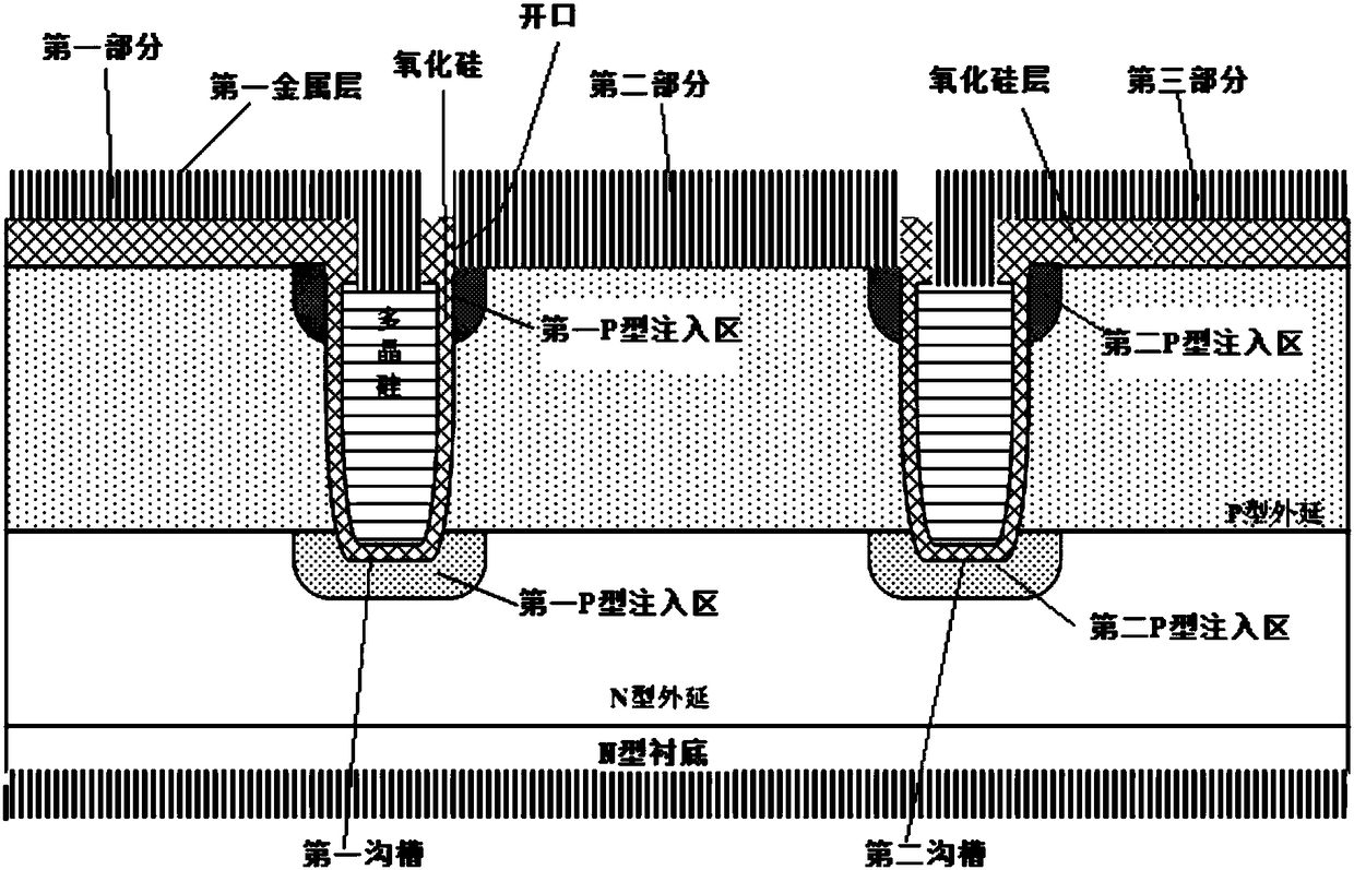
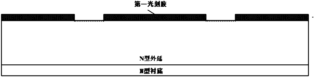
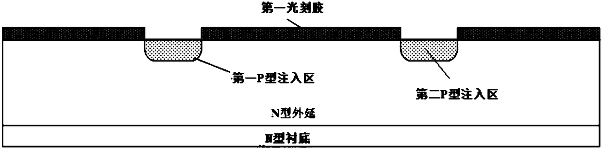
[0031] The fabrication method of vertical double diffused field effect transistor provided by the present invention can be applied to power devices, such as the fabrication of injection epitaxial vertical double diffused field effect transistor (VDMOS), further, the fabrication method of vertical double diffused field effect transistor provided by the present invention It is mainly suitable for N-channel vertical double-diffused field effect transistors. As a preferred implementation scheme, the fabrication method of...


PUM


Abstract

A vertical double-diffused field effect transistor includes an N-type substrate, an N-type epitaxial layer formed on the N-type substrate, first and second P-type implanted regions formed on the surface of the N-type epitaxial layer, a P-type epitaxial layer formed on the N-type epitaxial layer and the first and second P-type implanted regions, first and second N-type implanted regions formed on the surface of the P-type epitaxial layer and corresponding to the first and second P-type implanted regions respectively, a silicon oxide layer formed in the P-type epitaxial layer and the first and second N-type implanted regions, first and second trenches passing through the silicon oxide layer and the first N-type implanted region and extending into the first and second P-type implanted regionsrespectively; silicon oxide formed in the inner walls of the first and the second trenches and connected with the silicon oxide layer, openings passing through the silicon oxide layer between the first and the second trenches and corresponding to the P-type epitaxial layer and the first and second N-type implanted regions, and polycrystalline silicon formed on the surface of the silicon oxide layer in the first and second trenches.

Description

【Technical field】 [0001] The invention relates to the technical field of semiconductor chip fabrication, in particular to a vertical double diffused field effect transistor (VDMOS) and a fabrication method thereof. 【Background technique】 [0002] The drain and source poles of the vertical double diffused field effect transistor (VDMOS) are respectively on both sides of the device, so that the current flows vertically inside the device, increasing the current density, improving the rated current, and the on-resistance per unit area is also small, which is a A very versatile power device. [0003] For power devices, there are two extremely important parameters, one is on-resistance and the other is breakdown voltage. From the application of power devices in electronic equipment, it is hoped that the on-resistance should be as small as possible, and the higher the breakdown voltage, the better. In order to withstand high voltages, power devices need to use very thick low-dope...

Claims


Application Information

Patent Timeline
Patent Type & Authority Applications(China)
IPC IPC(8): H01L29/78H01L21/336H01L29/06
CPCH01L29/0607H01L29/66712H01L29/7802
Inventor 不公告发明人
Owner SHANGHAI XINLONG SEMICON TECH CO LTD
Why Eureka
Try Eureka