A kind of rc-igbt device and preparation method thereof

A device and semiconductor technology, applied in the field of reverse conduction insulated gate bipolar transistor devices and their preparation, can solve the problems of poor reverse recovery ability of diodes, uneven current distribution in drift region, uneven heat distribution, etc., and achieve improved Latch-up resistance, optimization of forward conduction characteristics, effects of avoiding latch-up effect

Active Publication Date: 2020-11-27
UNIV OF ELECTRONICS SCI & TECH OF CHINA
View PDF4 Cites 0 Cited by
  • Summary
  • Abstract
  • Description
  • Claims
  • Application Information

AI Technical Summary

Problems solved by technology

[0004] In view of the above, the present invention aims at the voltage snapback (VoltageSnapback) existing in the traditional silicon-based RC-IGBT, the conduction voltage drop increases, the current distribution in the drift region is uneven, the heat distribution is uneven, and the reverse recovery capability of the diode is poor. Problem, a RC-IGBT device with a heterojunction structure and its preparation method are proposed. In the traditional RC-IGBT device, semiconductor materials with different band gaps are used, so that the band gap of the material in the collector short-circuit region is larger than that of the corresponding The forbidden band width of the contacted semiconductor material forms a heterojunction structure with rectification characteristics, thereby suppressing the voltage foldback phenomenon, optimizing the current distribution and thermal distribution in the drift region, and improving the reverse recovery and reliability of the device

Method used


Image

  • A kind of rc-igbt device and preparation method thereof
  • A kind of rc-igbt device and preparation method thereof
  • A kind of rc-igbt device and preparation method thereof

Examples


Embodiment 1

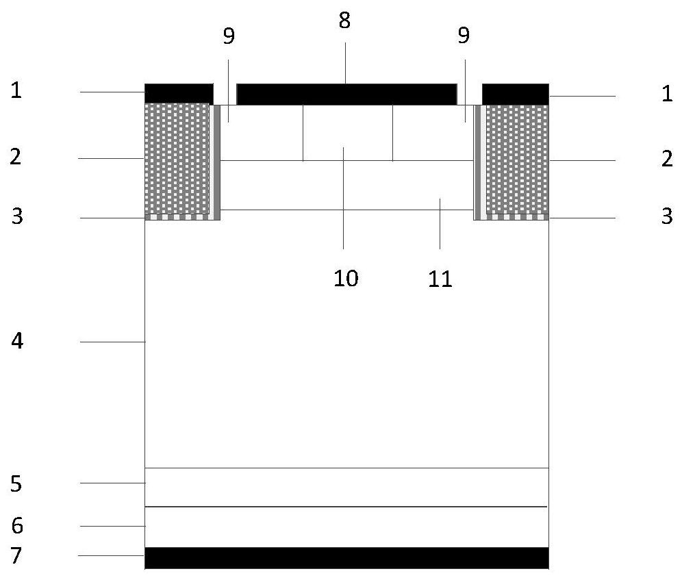
[0057] An RC-IGBT device whose cell structure is as follows Figure 4As shown, it includes: an N-type silicon drift region 4, an emitter structure and a gate structure located on the upper layer of the N-type silicon drift region 4, and a collector structure located on the lower layer of the N-type silicon drift region 4; the emitter structure includes a metal emitter Pole 8, N+ silicon emitter region 9, P+ silicon contact region 10 and P-type silicon base region 11, the P-type silicon base region 11 is located at the top of the N-type silicon drift region 4, and the N+ silicon emitter region 9 is located at the top of the P-type silicon On both sides of the top of the base region 11, the P+ silicon contact region 10 is located between and connected to the N+ silicon emitter region 9, and the metal emitter 8 is located on the upper surface of the N+ silicon emitter region 9 and the P+ silicon contact region 10; The gate structure includes a metal gate electrode 1, polysilicon ...

Embodiment 2

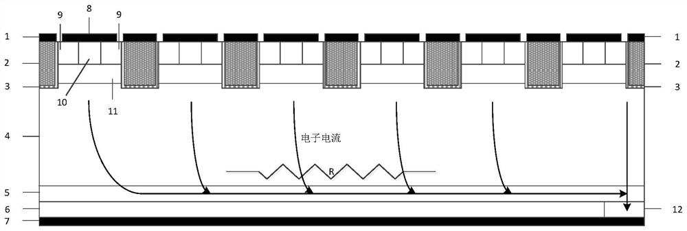
[0061] Compared with Embodiment 1, this embodiment differs in that: the number of P-type silicon carbide collector short-circuit regions 6 and N-type silicon carbide collector short-circuit regions 13 is different; in this embodiment, the N-type silicon carbide collector short-circuit regions 13 and The number of P-type silicon collector regions 6 is not less than two, and a plurality of N-type silicon carbide collector short-circuit regions 13 and a plurality of P-type silicon collector regions 6 are arranged at intervals, such as Figure 5 shown.

[0062] Compared with Example 1, due to the position away from the collector short-circuit area, the current needs to pass through a lateral resistance to reach the collector short-circuit area, and because the Si / SiC heterojunction is evenly distributed at the metal collector 7 and the interval is small, reducing The resistance value of the lateral resistance formed by the RC-IGBT above the P-type silicon collector region 6 is red...

Embodiment 3

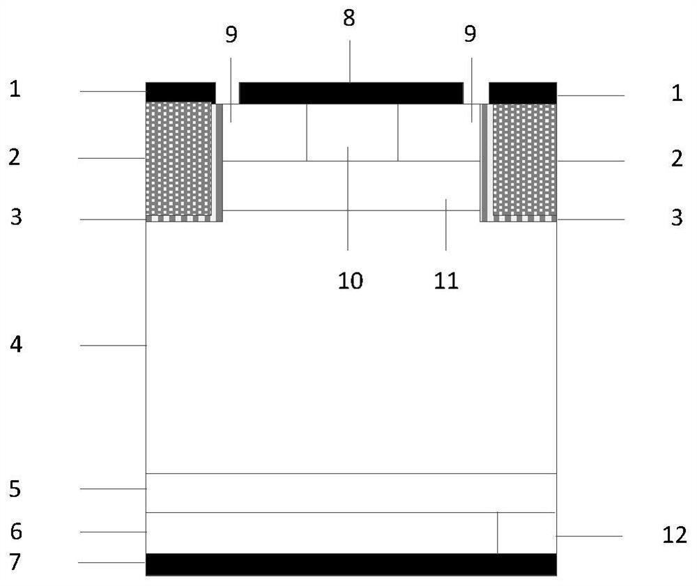
[0064] The difference between this embodiment and Embodiment 1 is that: the N-type silicon carbide collector short-circuit region 13 is formed by gradient doping; in this embodiment, the gradient doping specifically refers to the N-type silicon carbide collector short-circuit region 13 The doping concentration gradually decreases from top to bottom (that is, the doping concentration is from the junction of the N-type silicon field resistance layer 5 and the N-type silicon carbide collector short-circuit region 13 to the N-type silicon carbide collector short-circuit region 13 and the metal collector short-circuit region. The direction of the interface of the electrode 7 gradually decreases).

[0065] Such as Figure 7 Shown is the energy band diagram of the n-Si / N-SiC heterojunction formed by the gradually doped N-type silicon carbide collector short-circuit region 13 and the N-type silicon field stop layer 5 . Compared with Embodiment 1, the additional electron barrier provi...


PUM

PropertyMeasurementUnit
thicknessaaaaaaaaaa
depthaaaaaaaaaa
widthaaaaaaaaaa

Abstract

The invention discloses an RC-IGBT device and a preparation method thereof, belonging to the technical field of semiconductor power devices. The present invention uses semiconductor materials with different bandgap widths in traditional RC-IGBT devices to form collector short-circuit regions. The characteristic heterojunction structure, so that a single cell structure can eliminate the voltage snapback phenomenon (Voltage Snapback) in the forward conduction process of the traditional RC-IGBT, and optimize the current distribution and heat distribution in the drift region, avoiding current concentration and Reliability issues caused by heat concentration, and improve the reverse recovery capability of the device. Further, semiconductor materials with different forbidden band widths are used to form the emission region, and the forbidden band width of the emission region is larger than that of the semiconductor material in contact with it, thereby improving the anti-latch capability of the device.

Description

technical field [0001] The invention belongs to the technical field of semiconductor power devices, in particular to a reverse conducting insulated gate bipolar transistor (Reverse Conducting Insulated Gate Bipolar Transistors, RC-IGBTs) device and a preparation method thereof. Background technique [0002] With the continuous expansion of the depth and breadth of the human industrial revolution, people are constantly facing various crises while enjoying the convenience brought by the fruits of industrialization. As the "blood" of industry, the sustainable utilization of energy resources has always been valued by countries all over the world. The increasing consumption of energy resources has also made people feel the "energy crisis". While seeking new energy as an alternative to fossil energy, people are also thinking about how to maximize energy utilization. Electric energy is the main energy that human beings can directly use, and the power system that manages electric ...

Claims


Application Information

Patent Timeline
Patent Type & Authority Patents(China)
IPC IPC(8): H01L29/739H01L21/331
CPCH01L29/66325H01L29/7393
Inventor 张金平邹华罗君轶赵倩刘竞秀李泽宏张波
Owner UNIV OF ELECTRONICS SCI & TECH OF CHINA
Why Eureka
Try Eureka