A kind of horizontal rc-igbt device and its preparation method

A device and lateral technology, applied in the field of lateral reverse conduction insulated gate bipolar transistor devices and their preparation, can solve the problems of large turn-on voltage drop, poor diode reverse recovery capability, etc., so as to improve the turn-on voltage drop, improve Latch-up resistance, the effect of improving compromised performance

Active Publication Date: 2021-02-12
UNIV OF ELECTRONICS SCI & TECH OF CHINA
View PDF6 Cites 0 Cited by
  • Summary
  • Abstract
  • Description
  • Claims
  • Application Information

AI Technical Summary

Problems solved by technology

[0006] In view of the above, the present invention aims at the problems of voltage snapback (VoltageSnapback), large turn-on voltage drop and poor diode reverse recovery ability of the traditional lateral silicon-based RC-IGBT, and proposes a lateral In the RC-IGBT device and its preparation method, semiconductor materials with different bandgap widths are used in the traditional lateral RC-IGBT device, so that the bandgap width of the material in the collector short-circuit region is greater than the bandgap width of the semiconductor material in contact with it, thereby Form a heterojunction structure with rectification characteristics, thereby optimizing the forward conduction characteristics, suppressing the voltage foldback phenomenon, and improving the reverse recovery characteristics and reliability of the diode operation of the device

Method used


Image

  • A kind of horizontal rc-igbt device and its preparation method
  • A kind of horizontal rc-igbt device and its preparation method
  • A kind of horizontal rc-igbt device and its preparation method

Examples


Embodiment 1

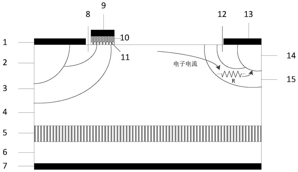
[0062] This embodiment provides as figure 2 The cell structure of the punch-through lateral SOI RC-IGBT device is shown, and its cell structure includes a substrate electrode 7, a P-type silicon substrate 6, an oxide layer 5, and an N-type silicon drift region 4 stacked sequentially from bottom to top. One side of the N-type silicon drift region 4 has an emitter structure and a gate structure, and the other side of the N-type silicon drift region 4 has a collector structure; the emitter structure includes a metal emitter 1, a P-type Silicon base region 3, P+ silicon contact region 2 and N+ silicon emitter region 8, the P-type silicon base region 3 is located in the N-type silicon drift region 4, and the P+ silicon contact region 2 and N+ silicon emitter region 8 are located side by side in the P The top layer of the type silicon base region 3, the metal emitter 1 is located on the upper surface of the P+ silicon contact region 2 and the N+ silicon emitter region 8; the gate s...

Embodiment 2

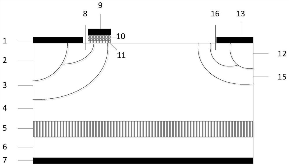
[0066] Such as image 3 As shown, the difference of this embodiment compared with Embodiment 1 is: through the change of process steps, the N-type silicon carbide collector short-circuit region 16 is arranged close to the emitter structure, while the P-type silicon collector region 12 is far away from the emitter structure settings.

[0067] In order to reduce the breakover voltage of the traditional lateral RC-IGBT, it is necessary to make the N-type silicon carbide collector short-circuit region 16 after the P-type silicon collector region 12 to increase the electron current resistance. Since there is no voltage foldback phenomenon in the device structure provided by the present invention, the N-type silicon carbide collector short-circuit region 16 can also be made before the P-type silicon collector region 12. At the same time, this improvement can further reduce the reverse operation of the device mode, and optimize the reverse recovery characteristics of the device in r...

Embodiment 3

[0069] Such as Figure 4 As shown, the difference of this embodiment compared with Embodiment 1 is that the depth of the N-type silicon carbide collector short-circuit region 16 is deepened by increasing the implant dose, prolonging the annealing time and other process controls.

[0070] In order to reduce the breakover voltage of the traditional lateral RC-IGBT, the depth of the N-type SiC collector short-circuit region 16 is controlled as shallow as possible to increase the electronic current path resistance. Since there is no voltage foldback phenomenon in the lateral RC-IGBT device provided by the present invention, and for the consideration of reducing the conduction voltage drop during reverse recovery, the depth of the N-type silicon carbide collector short-circuit region 16 can be deepened to further optimize the present invention. Invention of the reverse recovery characteristics of the device in the reverse mode of operation.


PUM

PropertyMeasurementUnit
thicknessaaaaaaaaaa
thicknessaaaaaaaaaa
thicknessaaaaaaaaaa

Abstract

The invention discloses a lateral RC-IGBT device and a preparation method thereof, belonging to the technical field of semiconductor power devices. In the present invention, semiconductor materials with different band gaps are used in the traditional lateral RC-IGBT device to form the collector short-circuit region, and the band gap of the material in the collector short-circuit region is greater than that of the semiconductor material in contact with it, thereby forming a collector short-circuit region with The heterojunction structure with rectification characteristics eliminates the voltage snapback phenomenon (Voltage Snapback) in the forward conduction process of the traditional lateral RC-IGBT, optimizes the forward conduction characteristics, improves the reliability of the device and the reverse recovery of the diode operation characteristics, and at the same time help to improve the voltage blocking capability of the device. Further, semiconductor materials with different forbidden band widths are used to form the emission region, and the forbidden band width of the emission region is larger than that of the semiconductor material in contact with it, thereby improving the anti-latch capability of the device.

Description

technical field [0001] The invention belongs to the technical field of semiconductor power devices, in particular to a lateral reverse conduction insulated gate bipolar transistor (Reverse Conducting Insulated Gate Bipolar Transistors, RC-IGBTs) device and a preparation method thereof. Background technique [0002] As the core of modern power systems, semiconductor power devices and their modules have been widely used in national defense construction, transportation, industrial production, medical and health and other fields. Since the first application of semiconductor power devices in the 1950s, the introduction of each generation of semiconductor power devices has enabled more efficient energy conversion and use. The history of semiconductor power semiconductor devices, that is, the history of the innovation of semiconductor power semiconductor devices. [0003] As one of the core devices of current semiconductor power devices, the insulated gate bipolar transistor not o...

Claims


Application Information

Patent Timeline
Patent Type & Authority Patents(China)
IPC IPC(8): H01L29/739H01L27/06H01L29/06H01L21/331
CPCH01L27/0629H01L29/0684H01L29/66325H01L29/7393
Inventor 张金平邹华罗君轶赵倩刘竞秀李泽宏张波
Owner UNIV OF ELECTRONICS SCI & TECH OF CHINA
Why Eureka
Try Eureka