A short-circuited anode soi LIGBT with an anode pinch-off slot

A technology of anode clamp and anode tank, which is applied in the direction of circuits, semiconductor devices, electrical components, etc., can solve the problems that affect the uniformity of device current distribution, large conduction voltage drop, and low anode hole injection efficiency, so as to eliminate voltage foldback Phenomenon, fast turn-off speed, effect of low conduction voltage drop

Active Publication Date: 2020-05-22
UNIV OF ELECTRONICS SCI & TECH OF CHINA
View PDF6 Cites 0 Cited by
  • Summary
  • Abstract
  • Description
  • Claims
  • Application Information

AI Technical Summary

Problems solved by technology

However, the introduction of the short-circuited anode structure makes the device switch between unipolar and bipolar modes when it is turned on, which brings the voltage foldback effect to the device and affects the uniformity of the current distribution of the device.
At the same time, the introduction of the short-circuited anode structure will make the anode hole injection efficiency low and the conduction voltage drop large.

Method used


Image

  • A short-circuited anode soi LIGBT with an anode pinch-off slot
  • A short-circuited anode soi LIGBT with an anode pinch-off slot
  • A short-circuited anode soi LIGBT with an anode pinch-off slot

Examples


Embodiment 1

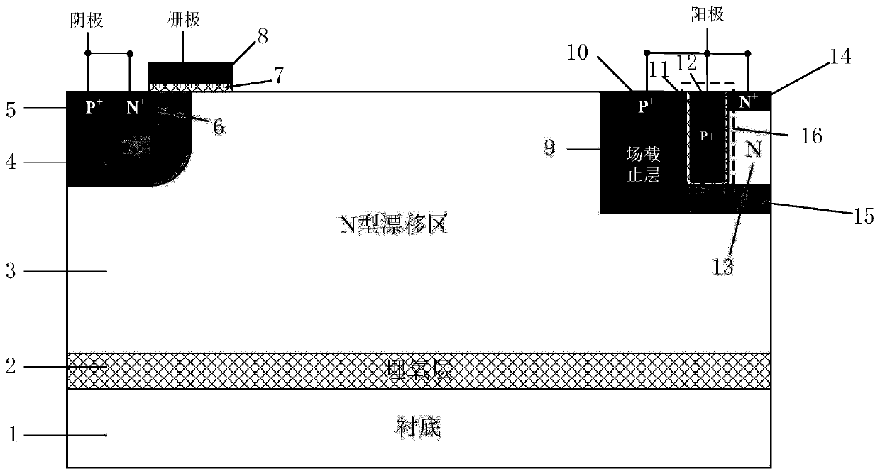
[0016] like figure 1 As shown, the structure of this example includes a P substrate 1, a buried oxide layer 2, and a top semiconductor layer stacked sequentially from bottom to top; the top semiconductor layer has an N-type drift region 3, and the device is along the In the lateral direction from one side to the other there are cathode structures, gate structures and anode structures in sequence.

[0017] The cathode structure includes a P well region 4, a P+ body contact region 5 located on the upper surface of the P well region 4 away from the anode structure, and an N+ cathode region 6 in contact with the P+ body contact region 5, and the P+ body contact region 5 and the N+ cathode region 6 have a common terminal as the cathode. There is a distance between the edges of the P+ body contact region 5 and the N+ cathode region 6 and the edge of the P well region 4 .

[0018] The gate structure is composed of an insulating medium 7 and a conductive material 8 on it, and the le...

Embodiment 2

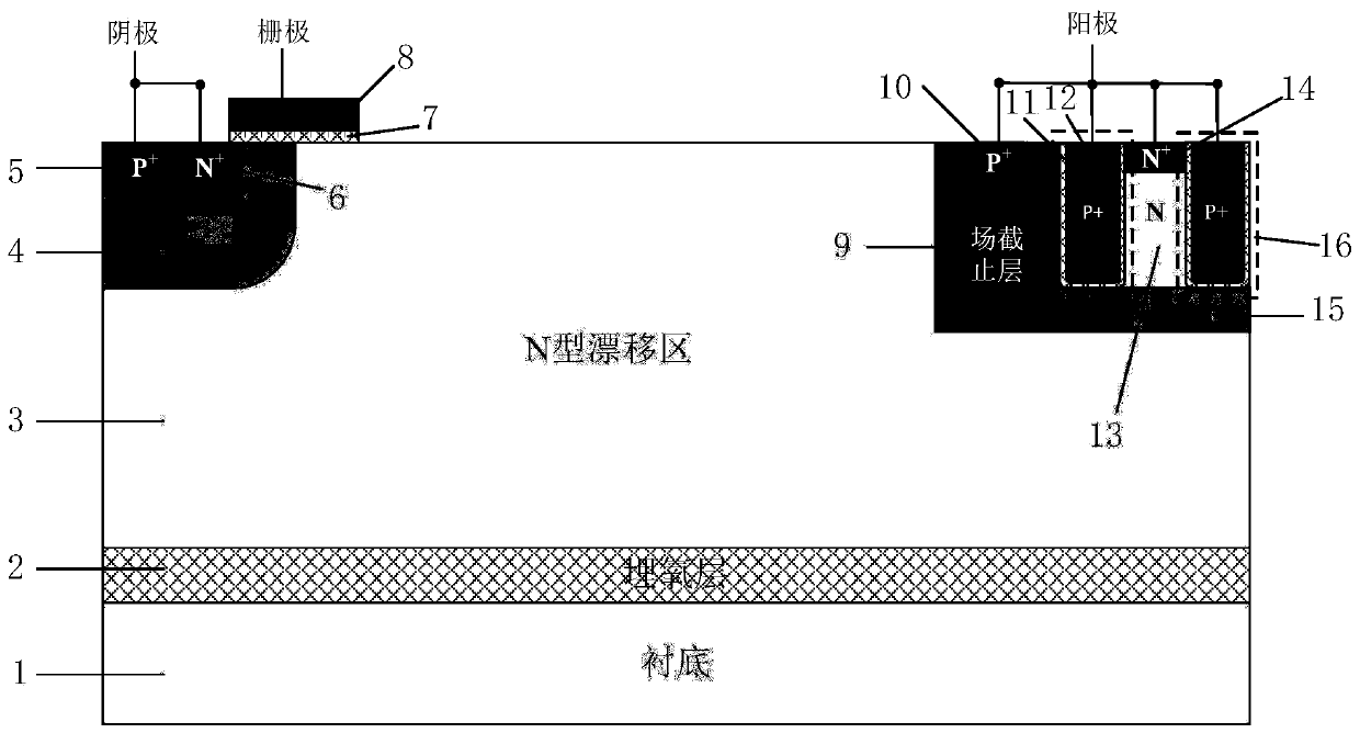
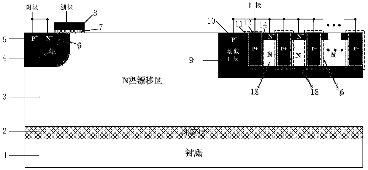
[0023] like figure 2 and 3 As shown, the difference between this example and Embodiment 1 is that there are two or more anode groove grid structures 16; the position of an anode groove 16 near the cathode side is as described in claim 1, and the rest of the anode groove 16 On the side away from the cathode structure, there are N-type doped regions 13 and N+anode regions 14 above the N-type doped regions 13 on both sides. Compared with Example 1, the design in this example uses two or more anode tanks, which enhances the depletion effect of P-type impurities in the anode tank on the low-concentration N-type doped region, and at the same time, increases the accumulation of more This not only enhances conductance modulation, further reduces the on-voltage drop, but also accelerates the extraction of electrons stored in the drift region, reducing turn-off time and turn-off loss.


PUM


Abstract

The invention belongs to the technical field of power semiconductors, and relates to a short-circuit anode SOI LIGBT (Lateral Insulated Gate Bipolar Transistor) with an anode pinch-off groove. Compared with the traditional short-circuit anode LIGBT, anode grooves connected with the anode potential are introduced at the anode end, a conductive material of the anode grooves comprises high-concentration P-type doping, and a low-concentration N-type doped region is introduced one side of each groove wall. When the device is turned off, the outer wall of each anode groove accumulates electrons, low-resistance channels are provided, the extractions of electrons in a drift region is accelerated, and the turn-off time and the turn-off loss are reduced. When the device is just turned on, a P-type impurity in the anode grooves enable the low-concentration N-type doped regions to be exhausted, the electrons are prevented from being extracted by the N+ anode, a voltage turning-back effect is eliminated, a conductivity modulation effect is enhanced at the same time, and the conduction voltage drop is reduced. The beneficial effects are that the short-circuit anode SOI LIGBT has high turn-off speed and lower loss compared with the traditional LIGBT; and the short-circuit anode SOI LIGBT eliminates the voltage turning-back phenomenon under a smaller transverse cell size compared with the traditional short-circuit anode LIGBT, and has lower conduction voltage drop at the same time.

Description

technical field [0001] The invention belongs to the technical field of power semiconductors, and relates to a short-circuited anode SOIL IGBT (Lateral Insulated Gate Bipolar Transistor, lateral insulated gate bipolar transistor) with an anode pinch-off groove. Background technique [0002] IGBT is a composite power semiconductor device composed of a metal oxide semiconductor field effect transistor (MOSFET for short) and a bipolar junction transistor (BJT for short). It combines the high input impedance of MOSFET and the conductance modulation of BJT. It has the advantages of low voltage, low driving power consumption, strong current capability, high withstand voltage characteristics, and good thermal stability. Among them, lateral IGBT (LIGBT) is easy to be integrated in silicon-based, especially SOI-based power integrated circuits. SOI-based LIGBT can completely eliminate the hole-electron injection of bulk silicon LIGBT substrate, and the use of dielectric isolation SOI t...

Claims


Application Information

Patent Timeline
Patent Type & Authority Patents(China)
IPC IPC(8): H01L29/739H01L21/331H01L29/06
CPCH01L29/0603H01L29/0611H01L29/0684H01L29/66325H01L29/7393
Inventor 罗小蓉杨洋魏杰欧阳东法王晨霞樊雕赵哲言孙涛邓高强
Owner UNIV OF ELECTRONICS SCI & TECH OF CHINA
Why Eureka
Try Eureka