A tunneling field effect transistor and its manufacturing method

A technology of tunneling field effect and manufacturing method, which is applied in the field of tunneling field effect transistor and its manufacturing, can solve the problems of high power consumption and the like, and achieve the effect of low power consumption

Active Publication Date: 2020-08-07
HUAWEI TECH CO LTD
View PDF3 Cites 0 Cited by
  • Summary
  • Abstract
  • Description
  • Claims
  • Application Information

AI Technical Summary

Problems solved by technology

[0004] However, the subthreshold swing (SS for short, also known as the subthreshold slope) value of the currently used tunneling field effect transistor is still unable to be lower than 60mV / dec, and the power consumption is relatively large.

Method used


Image

  • A tunneling field effect transistor and its manufacturing method
  • A tunneling field effect transistor and its manufacturing method
  • A tunneling field effect transistor and its manufacturing method

Examples


Embodiment Construction

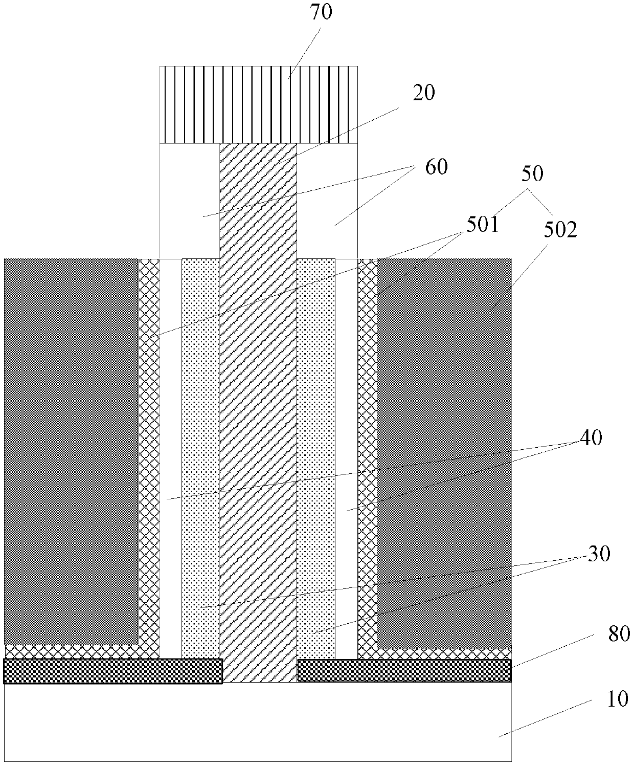
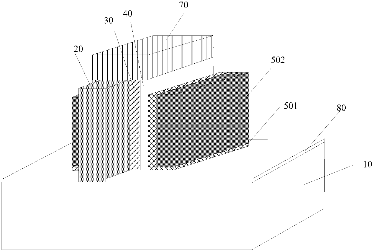
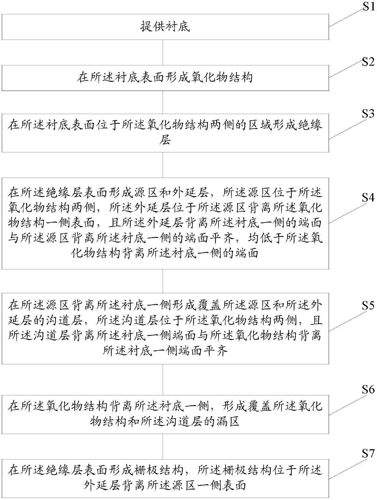
[0064] An embodiment of the present invention provides a tunneling field effect transistor, including:

[0065] Substrate;

[0066] an oxide structure, the oxide structure is located on the surface of the substrate;

[0067] an insulating layer, the insulating layer is located on the surface of the substrate and located on both sides of the oxide structure;

[0068] The source region is located on the surface of the insulating layer and on both sides of the oxide structure, and the end face of the source region facing away from the substrate is lower than the end face of the oxide structure facing away from the substrate;

[0069] an epitaxial layer, the epitaxial layer is located on the surface of the insulating layer, and is located on the surface of the side of the source region away from the oxide structure, and the end face of the epitaxial layer on the side away from the substrate is flush with the end face of the source region on the side away from the substrate;

[0...


PUM

PropertyMeasurementUnit
thicknessaaaaaaaaaa

Abstract

A tunneling field effect transistor and a manufacturing method thereof, in which the source region (30) is located on both sides of an oxide structure (20), and the epitaxial layer (40) is located on the source region (30) away from the oxide structure ( 20) On one surface, the gate structure (50) is located on the surface of the epitaxial layer (40) away from the source region (30), so that the electric field direction of the gate of the tunneling field effect transistor is consistent with the electron tunneling direction, and the value of the source region The tunneling efficiency of the carriers in the band to the conduction band of the epitaxial layer is high, which can generate a steep sub-threshold swing, which in turn makes the sub-threshold swing of the tunneling field effect transistor lower than 60mV/dec, and the power consumption smaller. Moreover, in the embodiment of the present invention, the epitaxial layer (40) is entirely located between the gate structure (50) and the source region (30), which increases the tunneling area between the epitaxial layer (40) and the source region (30), The subthreshold characteristic of the tunneling field effect transistor is further improved, and the subthreshold swing value of the tunneling field effect transistor is reduced.

Description

technical field [0001] The invention relates to the technical field of semiconductor devices, in particular to a tunneling field effect transistor and a manufacturing method thereof. Background technique [0002] As the size of metal-oxide-silicon field effect transistors continues to shrink, especially when the feature size of the device enters the nanowire scale, the negative impact of the short channel effect of the device becomes more and more obvious. The subthreshold slope of traditional MOSFET devices cannot be reduced synchronously with the reduction of device size due to the theoretical limitation of thermoelectric potential KT / q, and its subthreshold leakage current also increases continuously with the decrease of threshold voltage. In order to overcome the increasing challenges faced by MOSFETs at the nanometer scale, new device structures and fabrication methods have become the focus of attention for small-scale devices. [0003] Tunnel field effect transistor (...

Claims


Application Information

Patent Timeline
Patent Type & Authority Patents(China)
IPC IPC(8): H01L29/78
CPCB82Y10/00H01L29/7391H01L29/775H01L29/0676H01L29/068H01L29/78H01L21/02293H01L21/31111H01L21/31144H01L29/66742H01L29/66977H01L29/78642H01L29/78696
Inventor 赵静张臣雄
Owner HUAWEI TECH CO LTD
Why Eureka
Try Eureka