Method for improving performance of AlTiSiN coating through low-negative bias high-energy Ar <+> etching cleaning
A negative bias, high-energy technology, applied in coating, metal material coating process, ion implantation plating, etc., can solve problems such as increasing power supply requirements, large cleaning negative bias, etc., to improve cutting performance and improve film base. The effect of bonding force, improved friction and wear resistance and cutting performance
- Summary
- Abstract
- Description
- Claims
- Application Information
AI Technical Summary
Problems solved by technology
Method used
Image
Examples
Embodiment 1
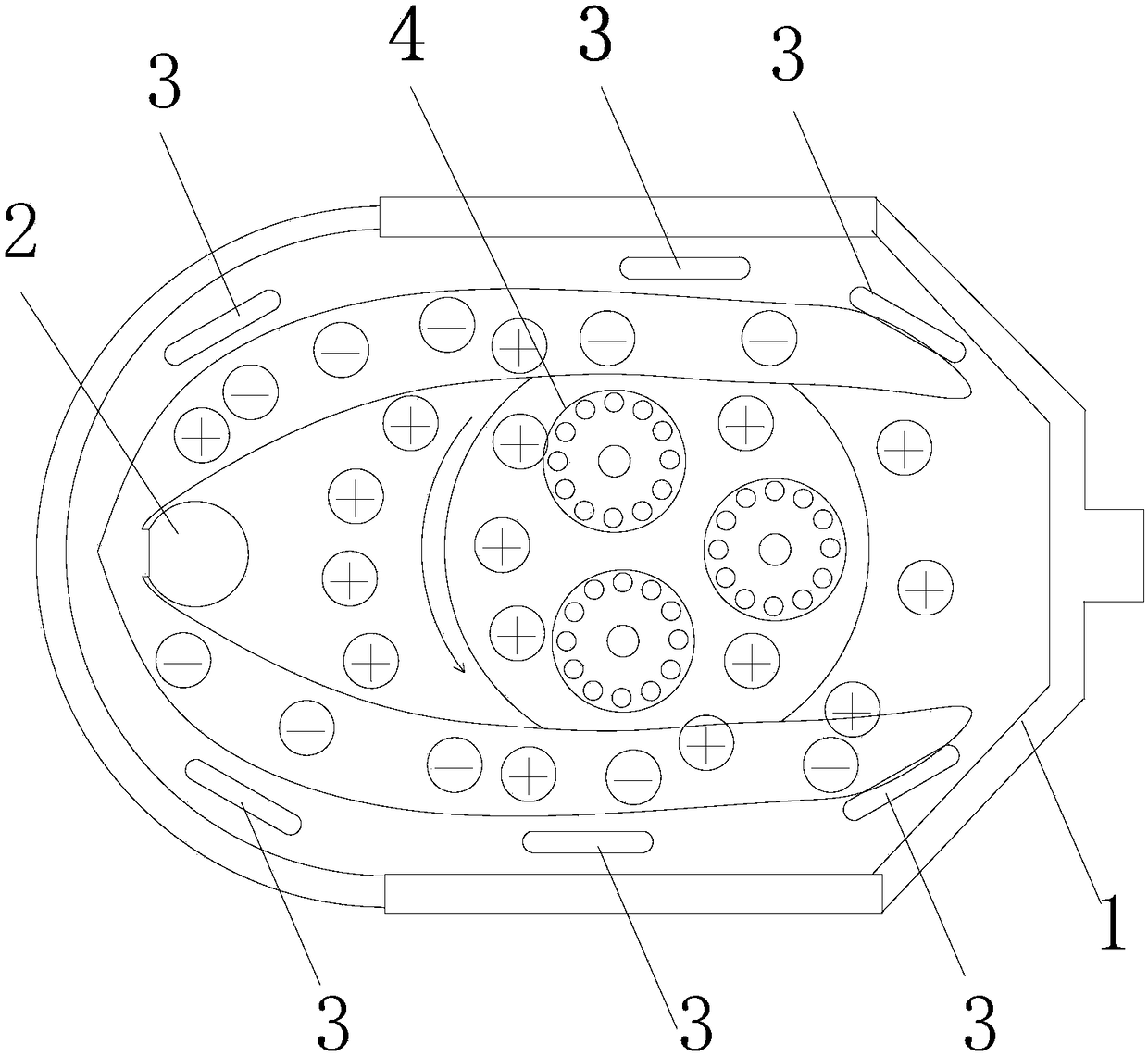
[0026] Such as figure 1 As shown, there are one columnar Ti target 2 for high-energy ion cleaning and six targets 3 for coating deposition distributed in the chamber 1 of the vacuum furnace in this embodiment. When the furnace reaches a high vacuum, the cylindrical Ti target 2 is turned on to ionize a large amount of Ti ions, and at the same time, argon gas is introduced to excite the Ar + Etching and cleaning the substrate, 4 in the figure is the workpiece.
[0027] When the vacuum degree in the furnace reaches 2.0×10 -4 At Pa, Ar gas with a purity of 99.999% was introduced and heated to 450°C. Turn on the cylindrical Ti target as a traction arc target, control the current during cleaning to 40A, and generate a large number of electrons. Turn on the circular auxiliary anode target to form positive and negative pull electron movement with the Ti target. Electrons collide with Ar gas in the furnace to produce high-density Ar + . The negative bias of the substrate is -180V...
Embodiment 2
[0033] The high-energy Ar of this embodiment + During the ion etching process, the arc cleaning current of the Ti column was controlled to be 70A, and the substrate cleaned by ion etching and the prepared coating were tested.
[0034] Other implementations are the same as in Example 1.
Embodiment 3
[0036] The high-energy Ar of this embodiment + During the ion etching process, the arc cleaning current of the Ti column was controlled to be 100A, and the substrate cleaned by ion etching and the prepared coating were tested.
[0037] Other implementations are the same as in Example 1.
[0038]The detailed cleaning and deposition process parameters of the coatings of each embodiment are shown in Table 1.
[0039] Table 1 Detailed cleaning and deposition process parameters of AlTiSiN coating
[0040]
[0041] After the samples of each embodiment are prepared, related tests are carried out, and the test results of the AlTiSiN coating are shown in Table 2.
[0042] Table 2 Test results of AlTiSiN coating
[0043]
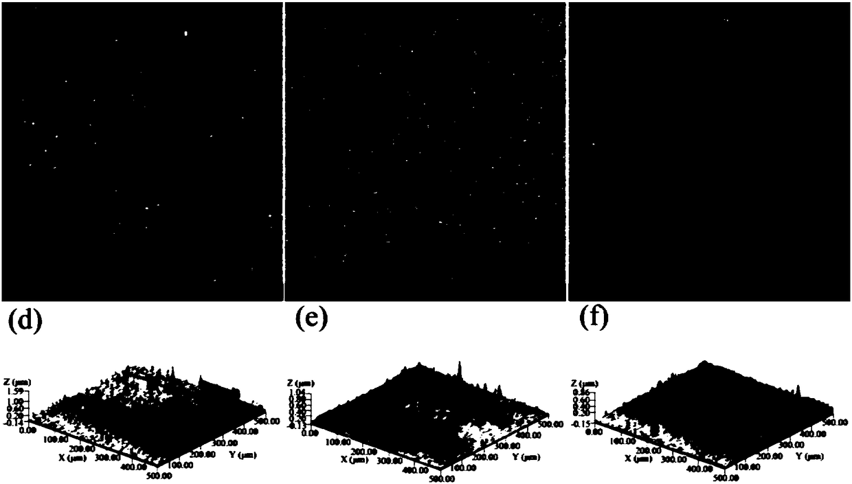
[0044] figure 2 Ar under different cleaning current conditions + Surface SEM and three-dimensional topography of the substrate after etching treatment. Depend on figure 2 (a) and (d), it can be found that when the cleaning current is 40A, the Ar + Afte...
PUM
 Abstract
Description
Claims
Application Information


