Growth method capable of effectively reducing silicon carbide epitaxial surface defects

A growth method and epitaxial growth technology are applied in the growth field that can effectively reduce the surface defects of silicon carbide epitaxy, and can solve the problems of low device production yield, many surface defects of SiC epitaxial wafers, hindering the promotion and application of SiC materials, etc. The effect of reducing surface defects and high promotion value

Inactive Publication Date: 2018-06-15
李哲洋
View PDF9 Cites 18 Cited by
  • Summary
  • Abstract
  • Description
  • Claims
  • Application Information

AI Technical Summary

Problems solved by technology

However, many defects in the substrate material will gradually diffuse or evolve into the epitaxial layer with the epitaxial growth, resulting in many surface defects on the Si

Method used


Image

  • Growth method capable of effectively reducing silicon carbide epitaxial surface defects
  • Growth method capable of effectively reducing silicon carbide epitaxial surface defects
  • Growth method capable of effectively reducing silicon carbide epitaxial surface defects

Examples


Embodiment 1

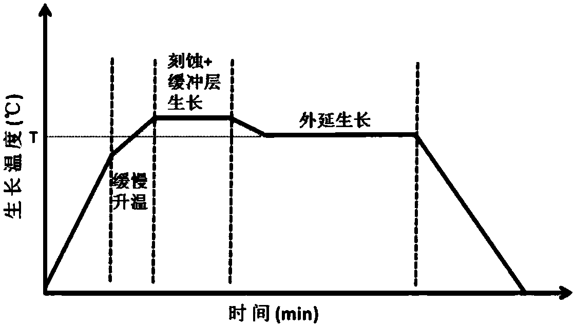
[0020] The provided silicon carbide film growth method using silane+propane+hydrogen chloride comprises the following steps:

[0021] Step 1: Select a silicon carbide substrate with a silicon surface that is 4° to the direction, and place the substrate in a graphite base after standard cleaning;

[0022] Step 2: Put the graphite base into the reaction chamber, replace the air with argon, pump the reaction chamber to a vacuum, and then pass hydrogen gas into the reaction chamber to keep the H 2 The flow rate is 160L / min, the pressure of the reaction chamber is 100mbar, and the reaction chamber is heated from room temperature to 1400°C at a fixed heating rate of 25°C / min by radio frequency heating; then the heating rate is reduced to 15°C / min, and the temperature is raised to 1580°C, constant temperature etching for 10 minutes;

[0023] The third step: pass silane (SiH 4 )+propane+(C 3 h 8 ) + hydrogen chloride (HCl) mixed gas, set the silane flow rate to 50 sccm, C / Si to 0...

Embodiment 2

[0027] The provided silicon carbide film growth method using silane+propane+hydrogen chloride comprises the following steps:

[0028] Step 1: Select a silicon carbide substrate with a silicon surface that is 4° to the direction, and place the substrate in a graphite base after standard cleaning;

[0029] Step 2: Put the graphite base into the reaction chamber, replace the air with argon, pump the reaction chamber to a vacuum, and then pass hydrogen gas into the reaction chamber to keep the H 2 The flow rate is 180L / min, the pressure of the reaction chamber is 150mbar, and the reaction chamber is heated from room temperature to 1400°C at a fixed heating rate of 30°C / min by radio frequency heating; then the heating rate is reduced to 15°C / min, and the temperature is raised to 1570°C, constant temperature etching for 11 minutes;

[0030] The third step: pass silane (SiH 4 )+propane+(C 3 h 8 ) + hydrogen chloride (HCl) mixed gas, set the silane flow rate to 50sccm, C / Si to 1....

Embodiment 3

[0034] The provided silicon carbide film growth method using silane+propane+hydrogen chloride comprises the following steps:

[0035] Step 1: Select a silicon carbide substrate with a silicon surface that is 4° to the direction, and place the substrate in a graphite base after standard cleaning;

[0036]Step 2: Put the graphite base into the reaction chamber, replace the air with argon, pump the reaction chamber to a vacuum, and then pass hydrogen gas into the reaction chamber to keep the H 2 The flow rate is 180L / min, the pressure of the reaction chamber is 150mbar, and the reaction chamber is heated from room temperature to 1400°C at a fixed heating rate of 30°C / min by radio frequency heating; then the heating rate is reduced to 15°C / min, and the temperature is raised to 1560°C, constant temperature etching for 12 minutes;

[0037] The third step: pass silane (SiH 4 )+propane+(C 3 h 8 ) + hydrogen chloride (HCl) mixed gas, set the silane flow to 100sccm, C / Si to 1.2, th...


PUM


Abstract

The invention mainly solves the technical problem, and provides a growth method capable of effectively reducing silicon carbide epitaxial surface defects. A buffer layer grows under the condition thata temperature is higher than an epitaxial growth temperature by adopting a low temperature and high temperature combined on-line in-situ substrate etching process. Based on a conventional chemical vapor deposition epitaxial furnace at the present, extension and evolution growth of defects on a silicon carbide substrate are reduced by improving the on-line in-situ etching process and a buffer layer growth process, so that surface defects of an epitaxial layer are effectively reduced, and a high-quality silicon carbide homoepitaxial wafer is obtained. As compatible with a conventional silicon carbide epitaxy process, the process disclosed by the invention is applicable to the conventional commercial single-wafer and multi-wafer type epitaxial furnaces, and is relatively high in popularization value.

Description

technical field [0001] The invention relates to a growth method capable of effectively reducing surface defects of silicon carbide epitaxy, which is suitable for single-chip epitaxy furnaces and planetary multi-chip epitaxy furnaces. Through the combination of low and high temperature in-situ etching substrate process and high temperature and low speed epitaxial process of growth buffer layer higher than the epitaxial temperature, the epitaxial defect density on the silicon carbide surface is effectively reduced, especially the defects that have a fatal impact on device performance. Controls such as triangles, carrot dislocations, falling objects, and large triangles, such as figure 1 with image 3 As shown, the epitaxial surface defect density can be changed from 2 / cm 2 reduced to 0.5 / cm 2 the following. Moreover, the method has simple technological process, is easy to operate, has good repeatability and consistency, and is suitable for mass production. Background techn...

Claims


Application Information

Patent Timeline
IPC IPC(8): C30B25/20C30B29/36
CPCC30B25/183C30B25/20C30B29/36
Inventor 李哲洋刘胜友
Owner 李哲洋
Why Eureka
Try Eureka