

Device and method for deposition of silicon-based polycrystalline silicon film
A polysilicon film and deposition technology, applied in chemical instruments and methods, polycrystalline material growth, crystal growth, etc., can solve the problems of poor control of gettering process, high cost of MFC, poor gettering effect, etc., and achieve film quality Good getter performance, reduced growth cost, and easy installation
- Summary
- Abstract
- Description
- Claims
- Application Information
AI Technical Summary
Problems solved by technology
Method used
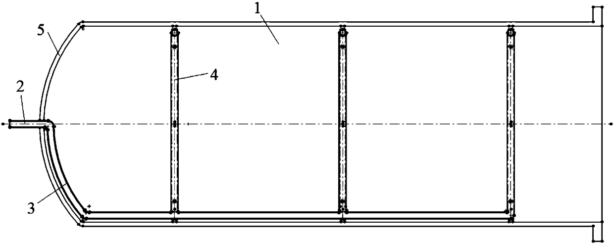
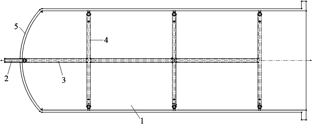
Image

Examples
Embodiment 1
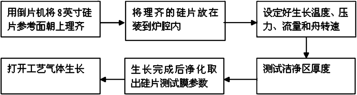
[0033] The present embodiment utilizes the method for depositing silicon-based polysilicon film by the device of the present invention to comprise the following steps: at first install the device of the present invention on the vertical furnace; Deposit a furnace with 150 8-inch silicon wafers; Arranging well, the reference side of the silicon wafer is facing up; put 150 product wafers into the vertical furnace, adjust the silane flow rate to 0.10SLM, the temperature in the deposition constant temperature zone is 710°C, the pressure is 550MT deposition, open the process gas growth, and the growth time is 60 minutes , Take out the silicon wafer after growth, the test film thickness is 5640 angstroms, the uniformity within the slice is 0.52% (required 10%), and the uniformity between 150 slices is 1.44% (required 10%). After taking out a piece of corrosion, observe the cleanness with a microscope The area is 75 microns (required 30 microns), which fully meets the requirements of ...
Embodiment 2
[0035] The present embodiment utilizes the method for depositing silicon-based polysilicon film of the present invention to comprise the steps: at first install the device of the present invention on the horizontal furnace; Deposit a furnace with 150 6-inch silicon wafers; Arranging well, the reference side of the silicon wafer is facing up; put 150 product wafers into the vertical furnace, adjust the silane flow rate to 0.10SLM, the deposition temperature to 710°C, the deposition pressure to 550MT, turn on the process gas growth, the growth time is 60 minutes, and the growth Take out the silicon chip afterward, the test film thickness is 6050 angstroms, the uniformity in the chip is 0.84% (requiring 10%), and the uniformity between 100 sheets is 1.55% (requiring 10%), take out a piece of corrosion and observe the clean area with a microscope as 55 microns (required 30 microns), fully meet the requirements of IC processing (the uniformity test mentioned in this embodiment is ...
Embodiment 3
[0037] The present embodiment utilizes the method for depositing silicon-based polysilicon film by the device of the present invention to comprise the following steps: at first install the device of the present invention on the vertical furnace; Deposit a furnace with 150 8-inch silicon wafers; Arranging well, the reference side of the silicon wafer is facing upward; put 150 product wafers into the vertical furnace, adjust the silane flow rate to 0.12SLM, the deposition temperature to 720°C, the deposition pressure to 500MT, turn on the process gas growth, the growth time is 60 minutes, and the growth Take out the silicon chip afterward, the test film thickness is 5860 angstroms, the uniformity in the chip is 0.66% (requiring 10%), and the uniformity between 100 sheets is 1.94% (requiring 10%), take out a piece of corrosion and observe the clean area with a microscope as 68 microns (requires 30 microns), which fully meets the requirements of IC processing (the uniformity test m...
PUM
 Abstract
Description
Claims
Application Information