
Crimping-type IGBT module with independently-formed chip and manufacturing method thereof

A chip and chip structure technology, which is applied in the field of high-power crimping IGBT modules and their preparation, can solve the problems of crimping IGBT modules, such as easy contamination, poor mechanical strength, and fretting wear, and improve assembly efficiency and assembly efficiency. Uniformity, avoiding fretting wear, and improving compressive strength

Active Publication Date: 2018-06-19
GLOBAL ENERGY INTERCONNECTION RES INST CO LTD +2
View PDF6 Cites 9 Cited by
  • Summary
  • Abstract
  • Description
  • Claims
  • Application Information

AI Technical Summary

Problems solved by technology

[0006] The technical problem to be solved by the present invention is that existing crimping type IGBT modules have defects such as easy contamination, complicated assembly, poor mechanical strength, and unavoidable fretting wear, and then provide a pollution-free, high-mechanical strength , easy to assemble, long service life, good reliability independently molded chip structure and its preparation method

Method used


Image

  • Crimping-type IGBT module with independently-formed chip and manufacturing method thereof
  • Crimping-type IGBT module with independently-formed chip and manufacturing method thereof
  • Crimping-type IGBT module with independently-formed chip and manufacturing method thereof

Examples


Embodiment 1

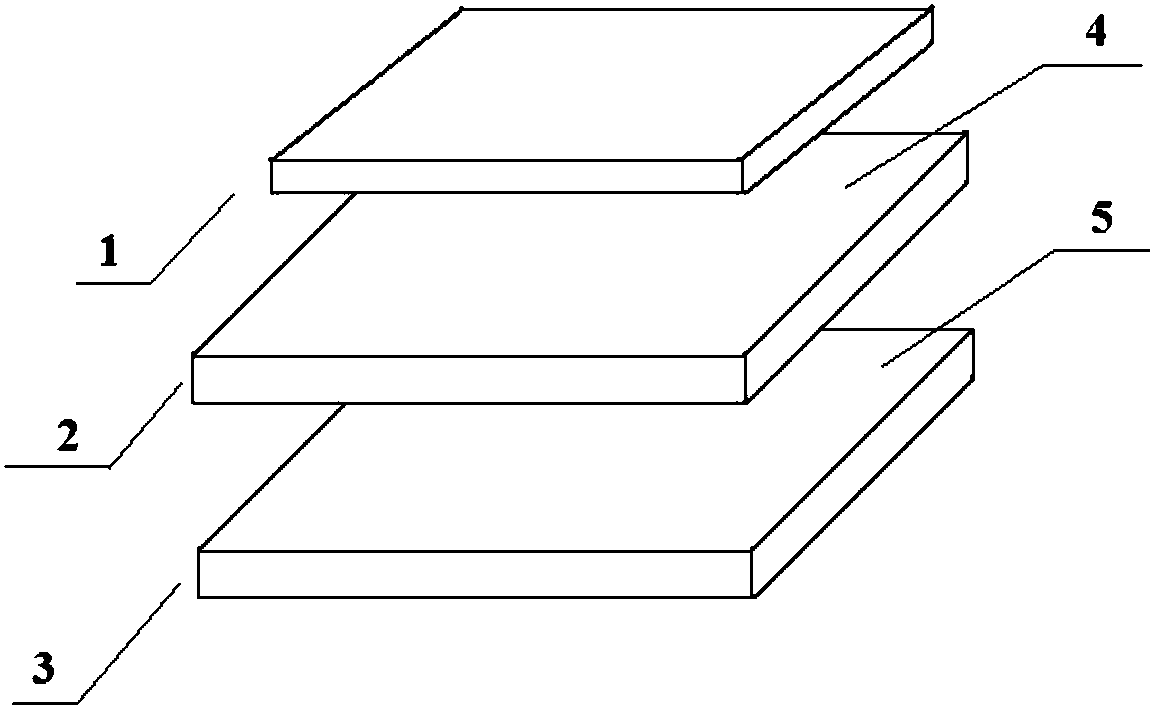
[0064] The crimping type IGBT module provided in this embodiment includes a cover plate, a chip assembly, a PCB board and a base in order from top to bottom. The chip assembly is composed of several chip units, each chip unit is composed of a chip structure and an insulating positioning member, and each chip structure is composed of a first conductive plane, a first sintering layer, a semiconductor chip, a second sintering layer, a second Composed of two conductive planes and an insulating shell, wherein the relative position of the chip sintered product composed of the first conductive plane, the first sintered layer, the semiconductor chip, the second sintered layer and the second conductive plane is as follows: figure 1 shown.

[0065] In this embodiment, the plastic frame is used as the insulating positioning member, and the surroundings of the chip structure are adhered to the top of the plastic frame. The top of the table is laminated; nano silver is used as the materia...

Embodiment 2

[0067] This embodiment provides a method for preparing the crimped IGBT module according to Embodiment 1 of the present invention, comprising the following steps:

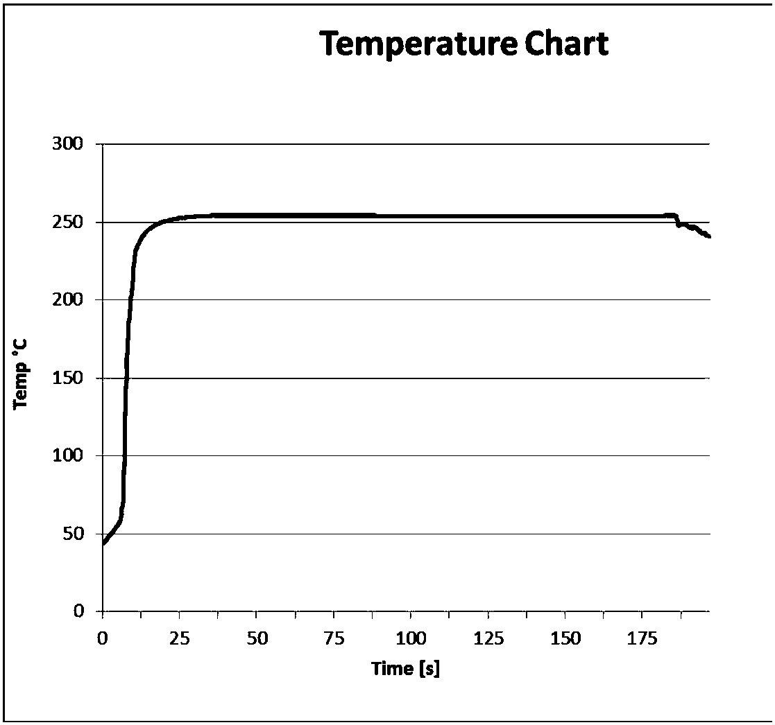
[0068] Preparation of chip sintered products: Get upper molybdenum sheet (bigger) and lower molybdenum sheet (lesser), and paste nano-silver film on one surface of upper and lower molybdenum sheet respectively, the thickness of described nano-silver film is 60 μ m, the nano-silver in film The content is 50wt%, and the upper and lower molybdenum sheets bonded with the nano-silver film are respectively subjected to pressure sintering at a sintering temperature of 110° C. and a pressure of 2 MPa to obtain a molybdenum sheet sintered with a nano-silver layer. Preferably, during the pressure sintering, the temperature is raised from room temperature to 110° C. at a rate of 5-10° C. / min, and then kept at a temperature of 15 minutes.

[0069] Vacuum ion sputtering is performed on the upper and lower surfaces of the semi...

Embodiment 3

[0078] The preparation method of the crimped IGBT module independently plastic-sealed by the chip product provided by this embodiment is roughly the same as that of Embodiment 2, and the difference is only in the following aspects:

[0079] The thickness of the nano-silver film used in this embodiment is 10 μm, the content of nano-silver in the film is 70wt%, the conditions of the first sintering are sintering temperature 140°C, pressurized pressure 6MPa, the conditions of the second sintering are sintering temperature 320°C, The pressurized pressure is 35MPa; preferably, when the first sintering and the second sintering are carried out, the temperature is raised from room temperature to the sintering temperature at a rate of 5-10°C / min, and then the first sintering is held for 10-15 minutes, and the second Keep warm for 20-60 minutes during sintering. During plastic sealing, this embodiment uses polyether ether ketone as the material of the plastic sealing mold.

[0080]The ...


PUM

PropertyMeasurementUnit
Melting pointaaaaaaaaaa
Thicknessaaaaaaaaaa
The average particle sizeaaaaaaaaaa

Abstract

The invention discloses a crimping-type IGBT module with an independently-formed chip and a manufacturing method thereof, which relate to the technical field of electrical element manufacturing and particularly relate to the technical field of high-power crimping-type IGBT module packaging. According to the chip structure provided in the invention, through carrying out insulated shell coating on the semiconductor chip sintered with a first conductive plane and a second conductive plane, the semiconductor chip can be protected to a maximum degree, the chip can be prevented from being polluted and damaged by the environment, the chip storage environment requirement severity can be reduced, and the risk of possible damages to the semiconductor chip during storage and packaging processes can be reduced to the minimum. The chip structure provided in the invention is convenient to store, the environment is loose, and the whole device reliability can be effectively improved. According to thecrimping-type IGBT module provided in the invention, the thermal contact resistance and the contact resistance are lower, the device reliability is high, the early failure rate is low, and when any parallel chip unit goes wrong, replacement can be carried out easily.

Description

technical field [0001] The invention belongs to the technical field of electrical components, and in particular relates to a high-power crimping type IGBT module with independently formed chips and a preparation method thereof. Background technique [0002] IGBT (Insulated Gate Bipolar Transistor), an insulated gate bipolar transistor, is the core device for energy conversion and transmission. At present, IGBT modules usually use soldering or crimping packaging. Among them, the press-fit IGBT module has dense chip layout, high power density, double-sided heat dissipation, and is easy to be connected in series. After being connected in series, it can effectively reduce the number of devices, simplify the main circuit structure, reduce control complexity, ensure device reliability, and use The device is more compact and lighter in weight, so it is widely used in high-voltage and high-power occasions such as power systems, electric locomotives, and smart grids. For example, ther...

Claims


Application Information

Patent Timeline
IPC IPC(8): H01L23/04H01L25/07H01L29/739H01L21/52
CPCH01L21/52H01L23/041H01L25/072H01L29/7393
Inventor 王亮林仲康田丽纷韩荣刚唐新灵石浩张朋李现兵张喆武伟
Owner GLOBAL ENERGY INTERCONNECTION RES INST CO LTD
Learn More